Article

Power Conversion Using Analytical Model of Cockcroft–Walton Voltage Multiplier Rectenna

1
Department of Aviation Sciences, Amman Arab University, Amman 11953, Jordan
2
Department of Electrical and Electronics Engineering, Universiti Teknologi PETRONAS, Seri Iskandar 31750, Malaysia
3
Department of Electrical Engineering, Engineering Faculty, The Hashemite University, Zarqa 13133, Jordan
4
Department of Fundamental and Applied Science, Universiti Teknologi PETRONAS, Seri Iskandar 32610, Malaysia
5
Department of Electrical Engineering, University of Gujrat, Punjab 50700, Pakistan
6
Department of Electrical and Electronics Engineering, University of Ilorin, Ilorin 240103, Nigeria
7
CHARUSAT Space Research and Technology Center, Patel Institute of Technology, Charotar University of Science and Technology, Gujarat 388421, India
*
Author to whom correspondence should be addressed.
Electronics 2021, 10(8), 881; https://doi.org/10.3390/electronics10080881
Submission received: 6 December 2020 / Revised: 21 January 2021 / Accepted: 28 January 2021 / Published: 7 April 2021
(This article belongs to the Special Issue RF Energy Harvesting and Wireless Power Transfer)

Abstract

:
A voltage multiplier rectenna is a combination of a voltage multiplier rectifier and an antenna used for the conversion of AC to DC. It is an essential part of the system of RF energy harvesting. Conventional rectennas are characterized by low conversion efficiency. This study presents an analytical novel mode designed for RF energy harvesting systems to study the voltage and current output of rectifier stages for efficiency optimization. The design contains a voltage multiplier rectification circuit with seven stages. The Schottky diode HSMS 285-C was selected for the circuit modeling voltage multiplier circuit. Advanced Design System (ADS) simulation was used to validate the equations of the theoretical model solved with MATLAB code. The fabricated system was tested for an input power range of 10 μW to 100 mW; the maximum output power is 0.2577 mW with maximum efficiency of 29.85%.

1. Introduction

Wireless communication has been growing rapidly over the last few years and has become an essential part of people’s daily lives. The importance of wireless communication lies in enabling users to be connected anywhere at any time. However, wireless networks are also known to emit a large amount of electromagnetic energy. Most recent works are trying to use this energy [1,2]. The radio frequency (RF) harvesting system is a basic unit in wireless power transmission [3,4,5,6]. The scientific and technological advancements associated with the use of RF energy harvesting technology has become more effective. There are different external ambient RF energy sources in this modern technology, with different resonance frequencies radiating RF signals in all directions. Some of those sources are television (TV), radio broadcast, mobile phone stations, cellular phones, and wireless local area network transceivers (LAN) [7]. RF energy harvesting system focuses on the continuous assembling of RF energy from ambient sources to provide necessary DC power to low-power devices [8]. RF harvesting system consists of a receiving circuit that receives the RF signal and converts it back to a DC signal. Rectennas are used as receivers in the RF harvesting system [9] by converting RF power, PRF into DC power, PDC at a certain frequency. The energy harvesting design has been proposed [10], as illustrated in Figure 1, which shows the schematic diagram of 43 RF energy harvester. This shows the connection of the antenna to an LC matching circuit, which is connected to a voltage multiplier rectifier. The antenna comprises a voltage source (Va), a radiation resistance (Ra), which produces an antenna current Ia. The LC impedance matching is located between the antenna and the rectifier. The impedance matching circuit contains passive elements such as capacitive or inductive reactance. The matching network results in a current, IL which passes through the resistance of voltage multiplier rectifier (RL) resultant in voltage (VL). The function of matching circuit is ensuring that maximum power is transferred from the antenna to the rectifier circuit. In the absence of the matching circuit, the RF power captured by the harvester antenna will be reflected, thus little power is realized at the rectifier. Several factors affect the efficiency of the RF harvesting system, these factors include [11]: The antenna’s efficiency, where the gain becomes smaller with decrease in size, and the power efficiency of voltage multiplier. The RF to DC conversion efficiency is described as the ratio of the DC output power (Pout) to the RF input power (Pin), where RF power is the power received by the antenna, and the DC power is the output power between terminals of the load resistor which is attached to the output of voltage multiplier. Where RF power is the power received by the antenna, and the DC power is the output power calculated between terminals of the load resistor attached to the output of voltage multiplier. The voltage multiplier (η) conversion efficiency can be found in (1):
η = DC   output   power   ( P out )   RF   input   power   P in
where PRF is the RF input power in the rectifying circuit. Reflected RF power is the dissipated power between the source and the voltage multiplier. Thus, some rectennas have low-efficiency (<15%) due to the small output power Pout produced by the rectifier. An analytical model to study the relations of the output voltage and current during different modes produced a good performance with good accuracy [12,13,14,15,16]. The parameters were designed without detaching the parasitic effects; consequently, the quantitative effect in the parasitic elements on the wireless RF harvester was not studied. This study presented the quantifiable effect of the rectifier elements on the performance of RF energy harvesters, with the effect of components which are used for impedance matching network. By studying the matching circuit quantitatively, the effect of each element on the performance of the harvester circuits tuned to improve the efficiency of the RF energy harvesting circuit. However, the model assumes steady-state conditions. To demonstrate the design, a harmonic simulation is used, besides a physical model fabrication. The key contribution in this paper is the design of an improved Cockcroft–Walton voltage multiplier rectifier based on an analytical model that can be used for power conversion applications. Further studies have been conducted on the voltage multiplier rectifier circuit by various authors [17,18,19,20,21,22,23,24,25,26,27].

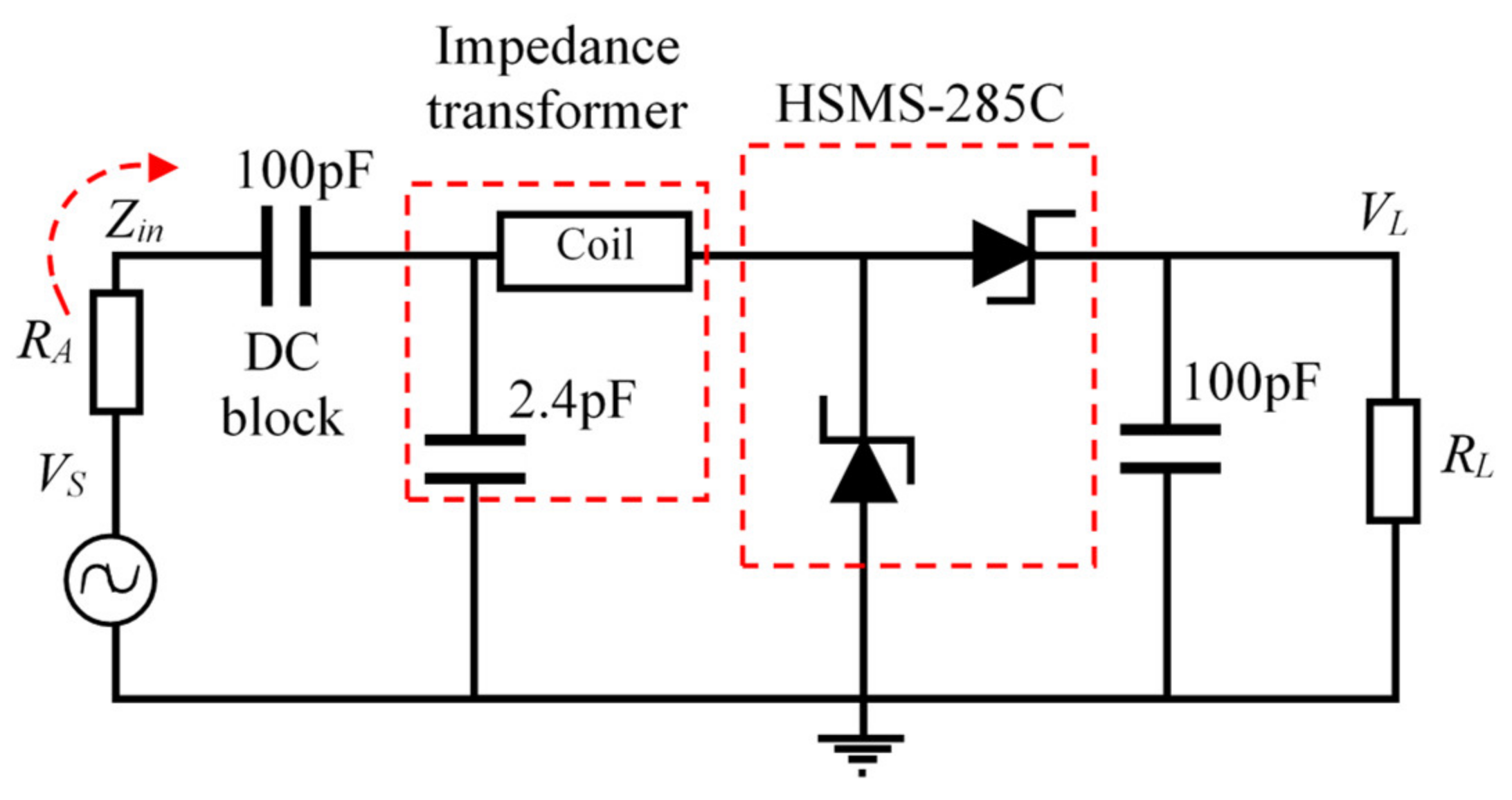
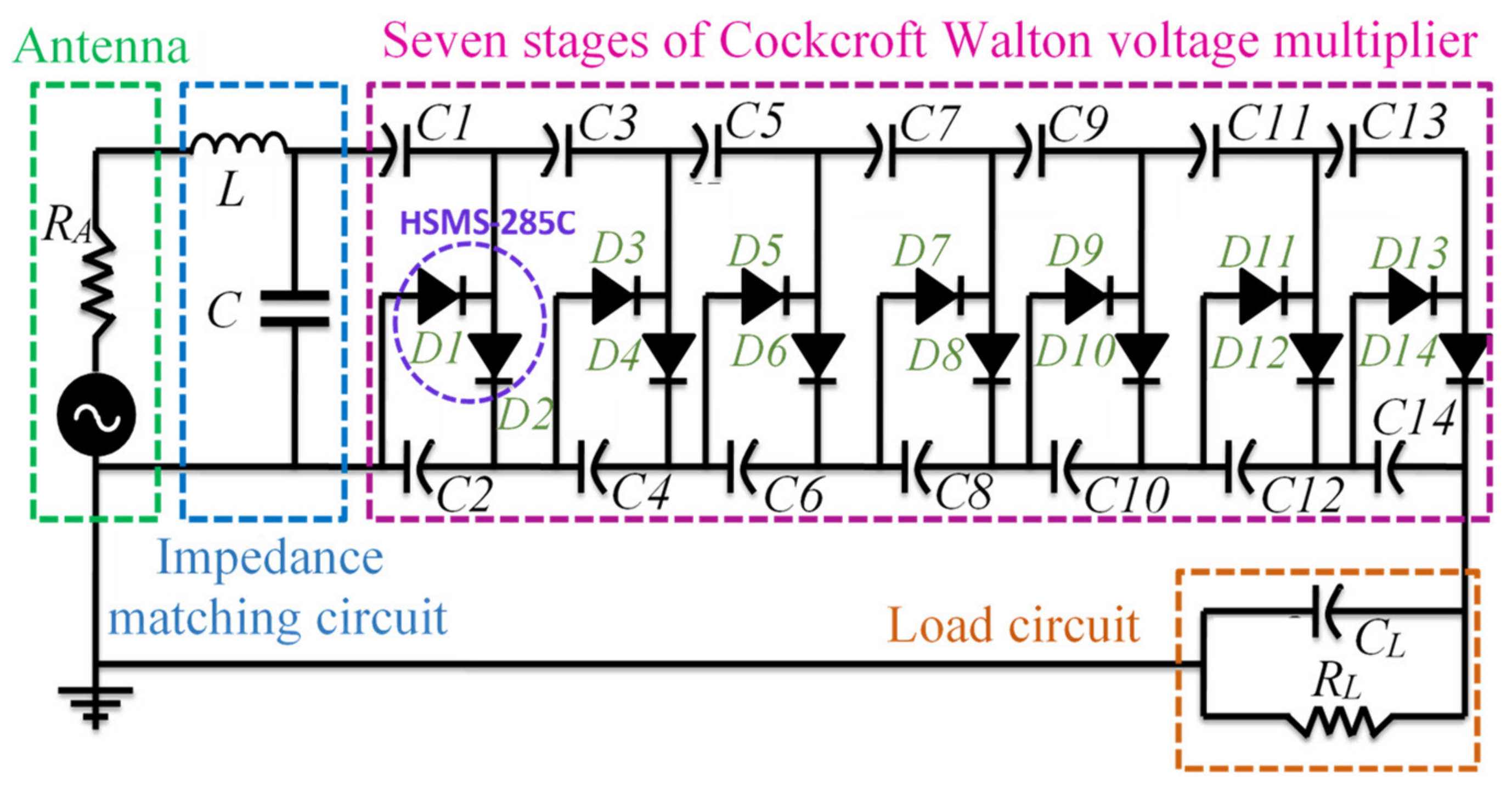
2. Methodology of Designing the Rectenna

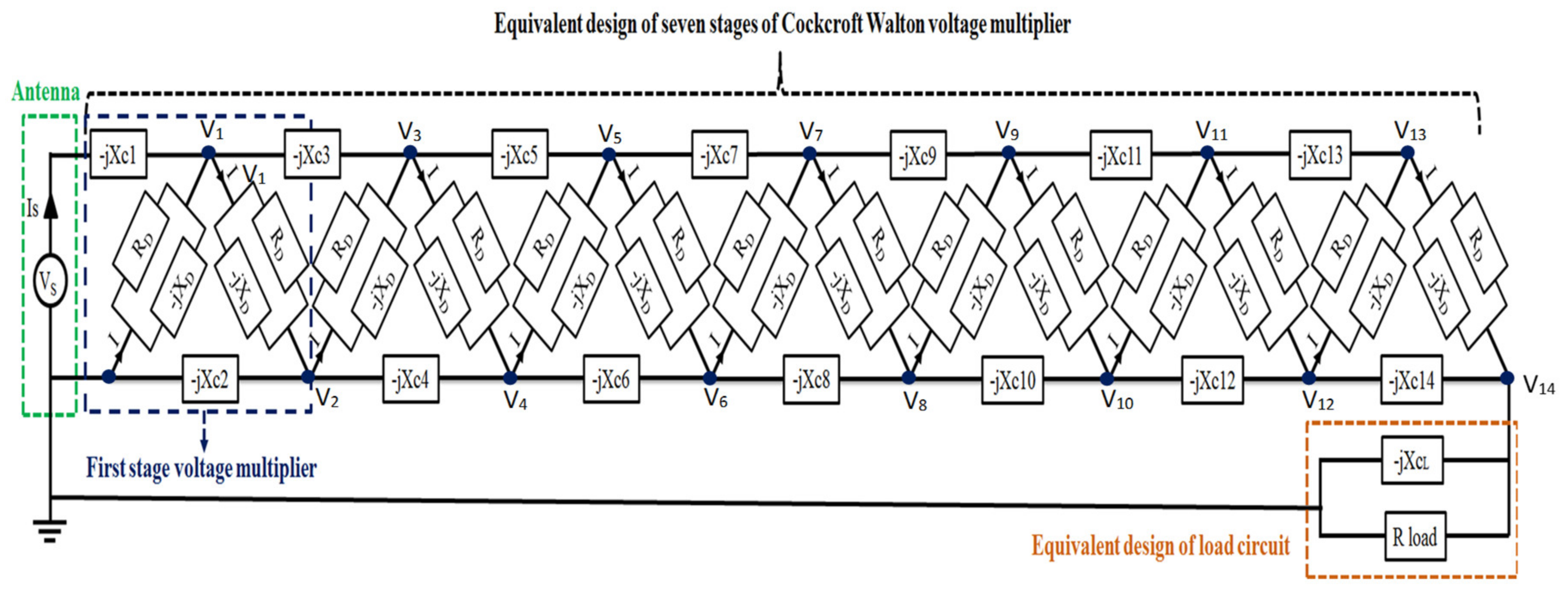
2.1. Linearized Analysis of Voltage Multiplier

The analytical model of a rectifying antenna is based on the linearization concept. The accurate techniques for determining the output results of rectifying circuits were given by the design. Figure 2 shows an RF harvester realized at 930 MHz by [28]. VS is the input voltage, RA is the antenna resistance, and RL is the load. After designing the linearized circuit as in Figure 2, the value of the output voltage VL is calculated using nodal analysis. The voltages at node VIN, VD and VL, are as shown in Figure 3.

2.2. Analytical Model of Cockcroft–Walton Voltage Multiplier Rectenna

Design consideration of the rectifying antenna is illustrated in this section for Cockcroft–Walton voltage multiplier circuit, as shown in Figure 4. The capacitor and resistor load values were calculated using the tuning tool in ADS software, as shown in Figure 4. The values of capacitors are selected based on the frequency value. The values of the L-network can be calculated using the Smith chart tool in ADS software.
The network schematic in Figure 5 shows the parameters of the matching network, where Zs is the impedance of the antenna, which is 50 Ω. Since the rectifier is a nonlinear circuit and its impedance value changes as a function of frequency and input power level, an input power value of 10 dBm was chosen since it has the best efficiency for seven stages, as stated in [29]. The network response was displayed by simulated real (red line) and imaginary (blue line) parts of the input impedance as a function of frequency. A matching network was designed to transform the impedance of the antenna (50 Ω) to the impedance of the voltage multiplier. The matching network consists of 8.33 nH and a 1.135 pF for inductor and capacitor, respectively. The capacitor was placed in parallel with the ports of the antenna, while the inductor was placed in series with the voltage multiplier. From the response of the network shown in Figure 5, it is clear that the proposed matching circuit will match the voltage multiplier impedance with the source at 900 MHz.
The design parameters for the proposed design are summarized in Table 1.
The original circuit, as shown in Figure 6, consists of the antenna, impedance matching and voltage multiplier. The main reason for choosing 7 stages of voltage multiplier is that the parasitic effect of the capacitor of each stage was increased, which accumulates and leads to a decrease in voltage gain [30,31,32]. The circuit was converted to a linearized circuit by replacing the diodes, the capacitor and inductor with their impedances, as shown in Figure 7. In general, the diode impedance is RD, capacitor impedance is -jXC, and inductor impedance is jXL. XC1–XC14 are the reactance with a value of 0.3 pF. XCL is the reactance with a value of 100 pF load capacitor. RL is the load resistance of the voltage multiplier [20].
To simplify the circuit and obtain the values of the output voltage and current (Vout) and (Iout), respectively, the circuit was divided into two modes, in which mode 1 and mode 2 were the negative and positives peaks, respectively.
(1)
MODE 1: During the negative half cycle of the first stage, when the first diode, D1, is ON state, the Id1 will pass through the diode D1. D2 is OFF at this stage, and the circuit behaves as an OPEN circuit. While in the second stage, D1 and D3 are in the ON state, while D2 and D4 are turned off. During stage three, D1, D3 and D5 are turned to the ON state, while D2, D4 and D6 are turned OFF. Until stage seven, “D1, D3, D5, D7, D9, D11 and D13” are turned ON, while “D2, D4, D6, D8, D10, D12 and D14” are turned OFF. Mode 1 is illustrated in Figure 8.
(2)
MODE 2: The same procedure is described in mode 2 since it represents the positive half cycle of the circuit. During the first stage, D2 is in the ON state while D1 is in the OFF state (the circuit is OPEN, and the diode D1 is OFF). During the second stage, D2 and D4 are turned ON while D1 and D3 are turned OFF. Until stage seven, “D2, D4, D6, D8, D10, D12 and D14” are turned ON and “D1, D3, D5, D7, D9, D11 and D13” are turned OFF. Mode 2 is represented in Figure 9.
The output voltage for each stage can be found during the positive peak mode when the diodes (D2–D14) are ON since the output voltage for each stage can be found at the end of each stage. An equation was derived for each stage, which results in a total of seven equations. As shown in Figure 10, the nodes “V2, V4, V6, V8, V10, V12, and V14” refer to the output voltage for stages 1, 2, 3, 4, 5, 6 and 7, respectively. Noting that V14 represents the output voltage of the circuit.
For linear circuit elements, the rule is V = I × Z, where V, I and Z are all complex variables. Impedances are added in series and in parallel in the same way as resistors, i.e., Zseries = Z1 + Z2, Zparallel = Z1||Z2 = (Z1 × Z2) ÷ (Z1 + Z2)
By applying Kirchhoff voltage law (KVL) and Kirchhoff current law (KCL) on the seven stages, Equations (2)–(8) were derived.
V 2 = V s + I s j X c + Z D
V 4 = V 2 j X c + Z D + j X c V 1 Z D
V 6 = V 4 j X c + Z D + j X c V 3 Z D
V 8 = V 6 j X c + Z D + j X c V 5 Z D
V 10 = V 8 j X c + Z D + j X c V 7 Z D
V 12 = V 10 j X c + Z D + j X c V 9 Z D
V 14 = V 12 j X c + Z D + j X c V 11 Z D
where Vs is the voltage source with a value of 0.762 V at 10 dBm.
jXL is the inductor impedance; its value is equal to 2πfL Ω;
jXC is the capacitor impedance; its value is equal to 1/(2πfC) Ω;
ZD is the impedance of the diode represented in the model by RD and −jXD; its value can be calculated using equations of diodes’ impedance.
The same principle applies to the values of the nodes output voltages for stages 1–7 in the first mode (V1V13), as shown in Equations (9)–(15):
V 1 = V s + I s Z D
V 3 = V 1 j X c + Z D + j X c V s Z D
V 5 = V 3 j X c + Z D + j X c V 2 Z D
V 7 = V 5 j X c + Z D + j X c V 4 Z D
V 9 = V 7 j X c + Z D + j X c V 6 Z D
V 11 = V 9 j X c + Z D + j X c V 8 Z D
V 13 = V 11 j X c + Z D + j X c V 10 Z D
Based on the previous equations, a general rule for n stages can be found from Equations (2)–(15);
V n = V 2 n 2 j X c + Z D + j X c V 2 n 3 Z D
The output current for any stage (In) can be found based on Equation (17);
I n = V n R n
where Rn is the load resistance. An increase in the number of stages will result in an increase in the value of the output voltage and a decrease in the value of the output current at the same time. For the mathematical expression of Cockcroft–Walton voltage Equations (2)–(15) were used for the simulation using MATLAB code as shown in Figure 10. The equations were written in MATLAB with input parameters for capacitors, frequency, ZD, jXL, jXC, input voltage and current Vs, Is, respectively. Values of V1 to V7 were obtained using Equations (9)–(15). The value of the output voltage is 1.50 V, and the value of output power is 57.1 µW for a load of resistance 50 KΩ. For the proposed circuit, the seven stages model has the best performance since it has a high ability to give the best output voltage. For the proposed design at the frequency of 900 MHz, the output voltage deteriorated after stage seven, as previously mentioned in earlier studies [32]. The reason for this trend is the increasing parasitic effect of the capacitors in each stage, which accumulates and leads to decreasing voltage gain [33].

3. Simulation Results of Cockcroft–Walton Multiplier Voltage Rectifier

HSMS-285x was selected because it has the largest efficiencies at the lowest powers due to its low turn-on voltage. The arrangement of the capacitors is in series with diodes. For rectified voltage applications, seven stages circuit has the best performance; for the frequency of 900 MHz, the output voltage declined from the seventh stage that was observed in recent works. The reason for this voltage deterioration is the increasing parasitic effect of the capacitors of each stage, which results in a decrease in the voltage gain.
Figure 11 shows the circuit design of the seven stages Cockcroft–Walton voltage multiplier rectenna. The circuit consists of an antenna (that generates a signal at 900 MHz), which is represented with an AC source in ADS, seven stages of rectifier circuit and load circuit.
Figure 12 illustrates the simulation results for the proposed design before and after adding the matching network. The value of the input voltage (Vin) is 0.762 V, and the output voltage before adding matching circuit is 2.384 V. The value of the output voltage after adding the matching network is 4.629 V. It was observed that the output is not accurately DC voltage; it is mostly an AC signal with a DC offset voltage. The increase in the output voltage is due to the addition of a matching circuit that operates as a detector for the circuit to confirm a good transformation of the power from the antenna to voltage multiplier.
The function of the voltage multiplier rectifier circuit is to increase the output voltage value, as shown in Figure 12. While in Figure 13, it is observed that the output current decreases after seven stages (with a value of 1.468 × 10⁻³ mA) before adding the matching network. The output current increased after adding the matching circuit due to the decrease of the dissipated output power as a result of the influence of the matching circuit.
Figure 14 illustrates that at 900 MHz, the input power rises to 64.8 µWatt, which is the power received by the antenna. It also observed that the output power decreased after the seventh stage to 1.7 µWatt. The dissipated power will increase by increasing the number of stages and elements. Using a matching circuit will increase the value of power to 29 µWatt, which is a positive indicator of the importance of adding the matching circuit to increase the efficiency of the voltage multiplier by decreasing the dissipated power as illustrated as well in [34,35].
Figure 15 shows the result of the simulation for the output voltage for stages Vin–V7. These results clearly show that there is an increase in the value of the Vout for every stage until the eighth stage, where the output voltage is almost the same due to the parasitic effect of the constituent capacitors of each stage. This trend continues until the increment becomes negligible. The results for Cockcroft–Walton voltage multiplier are presented in Table 2. It is observed that the output power increased for all the power input values. Based on equation 18, the output current increased, leading to an increment in the ripple voltage:
V r i p p l e = I o × N 2 + N 2 8 f C
where Io is the output current, N is the number of voltage multiplier stages, f is the resonance frequency, and C is the value of the capacitor. As a smaller ripple voltage is preferable, a smaller output current ensures that the output voltage signal is closer to the DC line.

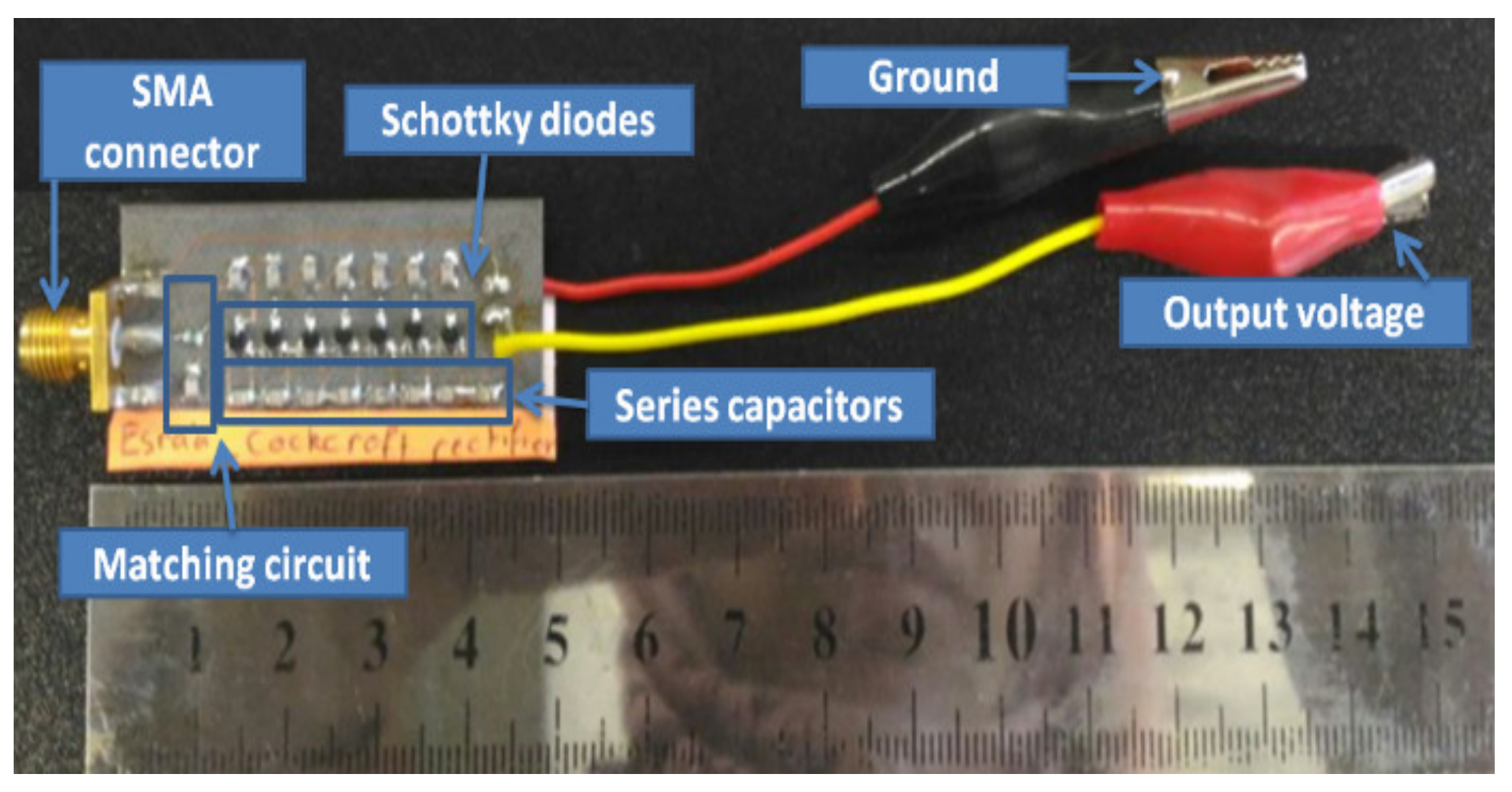
4. Fabrication of Cockcroft–Walton Multiplier Voltage Rectifier

EAGLE software, which is a schematic software used for PCB design, was used to design the voltage multiplier rectifier circuits for the purpose of rectifier prototyping. Figure 16 shows the circuit schematic diagram with the computed distance between the voltage rectifier elements. The dimension of the Cockcroft–Walton rectifier circuit is 45 × 18 mm, as shown in Figure 17. The components of the circuit, such as the SMA connector, matching circuit, Schottky diodes, series capacitors and the output terminals, are highlighted in the diagram. Roger 5880 was chosen for ground plane prototyping because of its advanced capabilities to boost the output voltage, as indicated by previous studies [22]. The mounting soldering technique was used to fix the elements of the voltage multiplier rectifier.
Figure 18 illustrates the testing setup for the proposed circuit. The circuit is connected to an RF signal generator, while its terminals are connected to the multimeter terminals to read the output values. The values of output voltage and current are 4.86 V and 68.73 µA, respectively.

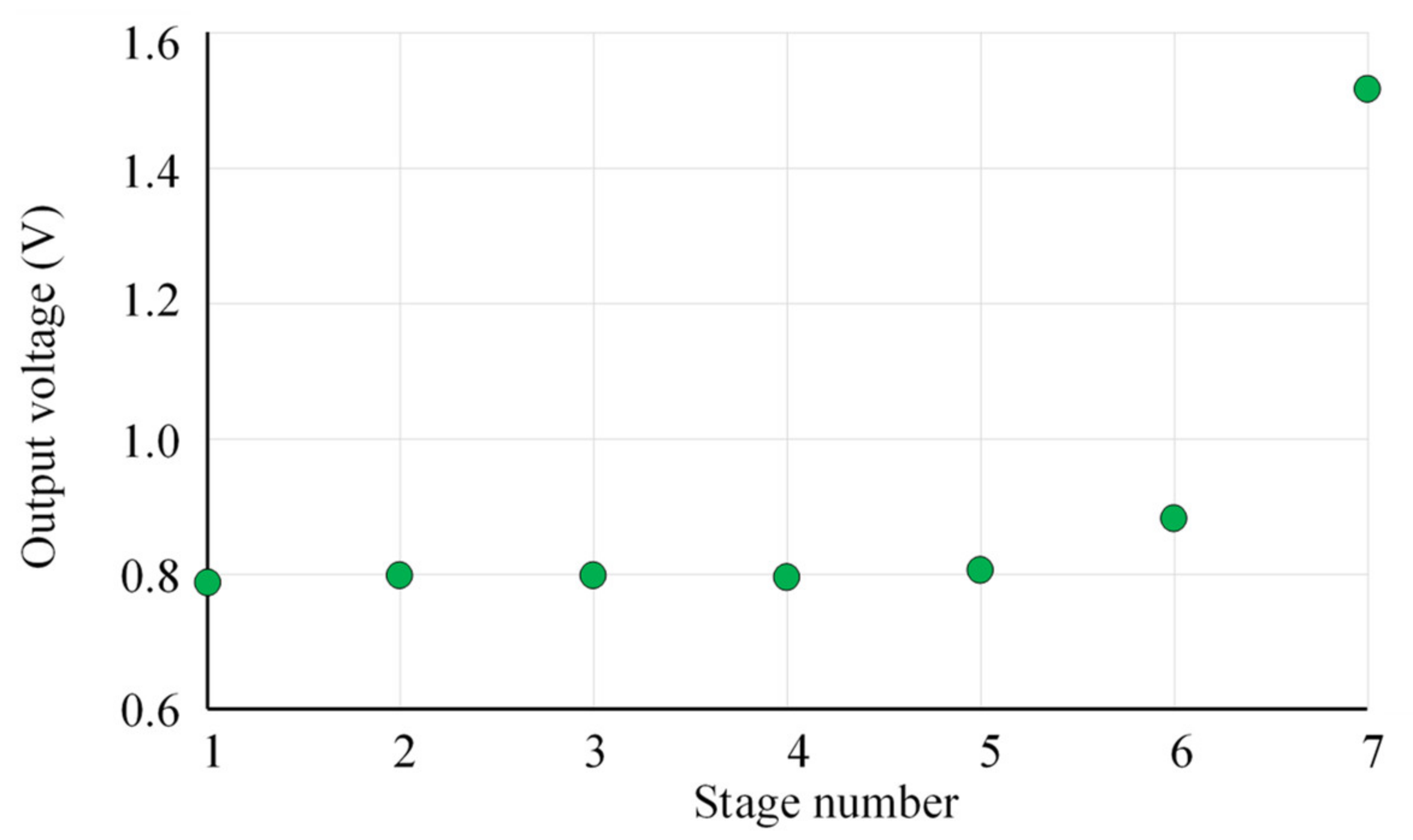
5. Results and Discussion

The output voltage was investigated by carrying out an analysis of the power input for the proposed design using the input power ranging from −20 dBm to 20 dBm. The values of the analytical, simulated, and measured output voltages are presented in Figure 19 for the rectifier models at 10 KΩ resistance load. As observed in the figure, the output power increased as the value of the input power increased.
As clearly shown in Table 3, there is a good correlation between the analytical, simulation and experimental results of the prototype. The minor difference in the output values, 4.86%, 4.88% and 9.77% for voltage, current, and power, respectively, is due to the change in the input power of the rectifier during the testing process due to internal inductance and the voltage drop across diodes.
The effect of the matching circuit is illustrated to prove its ability to decrease the reflected power between the antenna and voltage multiplier rectifier by increasing the value of output power of the circuits at the range of input power. The output voltage increased by 64.02%. As the load resistance increases, the output DC voltage also increases. The rate of increase of the output voltage was higher at the lower value of resistance, as illustrated in [36]. Figure 20 shows the output voltage versus load resistance at 900 MHz. The efficiency is summarized in Figure 21 for power input range −20 to 20 dBm. Higher power input results in higher efficiency [17,18,19,20,21,23,24].
Table 4 shows a comparison of this study with previous advanced research results that were conducted around 900 MHz frequency. The comparison is based on the circuit design and its output results. In [37], a six-stage Dickson multiplier was designed using Schottky diode to achieve a maximum output power of 50.28 mW, while a maximum output voltage of 1.6 V resulted in an efficiency of 54% by [38]. In [39,40], a good output was achieved, but the circuit’s profile was large, while other studies achieved less output voltage and efficiency. Holistically, compared to other studies, the proposed rectenna displays superior output voltage, power, and efficiency with a smaller size.

6. Conclusions

Since the effects of major parasitic elements on a wireless RF harvester performance are known, wireless RF harvesters capable of harvesting low ambient RF power levels can be realized. This study presents a novel analytical model for Cockcroft–Walton voltage multiplier for harvesting applications. The fabrication and testing of the complete RF energy harvesting system were discussed. The proposed design was tested at an input power level of–20 to 20 dBm with a resonance frequency of 900 MHz. A linearized mathematical model was also built for the voltage multiplier rectifier circuit. There is good agreement between the results of the developed mathematical expression and the simulation, indicating a good fit of the model. The minor difference between simulation and measurement results from the soldering effects when mounting the elements to the PCB and the nonlinearity characteristics of the diode. The results and discussion show that the designed rectifier circuit operates well at the targeted frequency and is suitable for use as an RF energy harvester.

Author Contributions

E.M.A. performed the analytic calculations, numerical simulations designed, performed the experiments, derived the models and analyzed the data. N.Z.Y. helped devised the project, the main conceptual ideas. O.A.S. helped in grammar check, prof reading, until simulation and equations validation. A.H.A.A. contributed to the final version of the manuscript. B.H.A. verified the analytical methods. S.I., O.I. and A.V.P. provided critical feedback and helped shape the research. All authors have read and agreed to the published version of the manuscript.

Funding

This work was partially supported by Research Institute of Autonomous System, Universiti Teknologi PETRONAS (UTP).

Acknowledgments

Authors are gratefully acknowledging Universiti Teknologi PETRONAS for research approval and financial support.

Conflicts of Interest

The authors declare no conflict of interest.

References

  1. Mandal, S.; Giri, S.K. Comparison of antennas for radio frequency energy harvesting in 0.2–2.4 GHz range. ICECT 2011, 1, 93–97. [Google Scholar]
  2. Ali, E.M.; Yahaya, N.Z.; al Assaf, A.H.; Alasali, F.; Patel, A.; Alqasem, B.H. Analysis and Maximizing RF Harvesting System based on Antenna Shapes for Aviation Applications. In Proceedings of the 2020 International Conference on Electrical Engineering and Control Technologies (CEECT), Swinburne, Australia, 10–13 December 2020; pp. 1–7. [Google Scholar]
  3. Kitazawa, S.; Ban, H.; Kobayashi, K. Energy harvesting from ambient RF sources. IMWS 2012, 34, 39–42. [Google Scholar]
  4. Sample, A.; Smith, J.R. Experimental results with two wireless power transfer systems. RWS 2009, 16–18. [Google Scholar]
  5. Papotto, G.; Carrara, F.; Palmisano, G.J. A 90-nm CMOS threshold-compensated RF energy harvester. IEEE J. Solid State Circuits 2011, 46, 1985–1997. [Google Scholar] [CrossRef]
  6. Ballo, A.; Bottaro, M.; Grasso, A.D.; Palumbo, G.J.E. Regulated charge pumps: A comparative study by means of verilog-AMS. Int. J. Sci. Eng. Res. 2020, 9, 998. [Google Scholar] [CrossRef]
  7. Piñuela, M.; Mitcheson, P.D.; Lucyszyn, S. Ambient RF energy harvesting in urban and semi-urban environments. IEEE Trans. Microw. Theory 2013, 61, 2715–2726. [Google Scholar] [CrossRef]
  8. Li, B.; Shao, X.; Shahshahan, N.; Goldsman, N.; Salter, T.; Metze, G.M. An antenna co-design dual band RF energy harvester. IEEE Trans. Circuits Syst. I Regul. Pap. 2013, 60, 3256–3266. [Google Scholar] [CrossRef]
  9. Visser, H.J.; Reniers, A.C.; Theeuwes, J.A. Ambient RF energy scavenging: GSM and WLAN power density measurements. EuMC 2008, 21, 721–724. [Google Scholar]
  10. Kundu, P.; Acharjee, J.; Mandal, K. Design of an efficient rectifier circuit for RF energy harvesting system. Int. J. Adv. Eng. Manag. 2017, 2, 94–97. [Google Scholar] [CrossRef]
  11. Waghamare, N.M.; Argelwar, R.P.J. High voltage generation by using Cockcroft-Walton multiplier. IJSETR 2015, 4, 256–259. [Google Scholar]
  12. Nimo, A.; Grgić, D.; Reindl, L.M.J.S. Optimization of passive low power wireless electromagnetic energy harvesters. Sensors 2012, 12, 13636–13663. [Google Scholar] [CrossRef]
  13. Tanzawa, T. An Analytical Model of AC-DC Charge Pump Voltage Multipliers. IEICE Trans. Electron. 2016, 99, 108–118. [Google Scholar] [CrossRef]
  14. Jia, P.; Yuan, Y.J. Analysis and implementation of LC series resonant converter with secondary Side clamp diodes under DCM operation for high step-up applications. J. Power Electron. 2019, 19, 363–379. [Google Scholar]
  15. Alghaythi, M.L.; O’Connell, R.M.; Islam, N.E.; Khan, M.M.S.; Guerrero, J.M. A High Step-Up Interleaved DC-DC Converter With Voltage Multiplier and Coupled Inductors for Renewable Energy Systems. IEEE Access 2020, 8, 123165–123174. [Google Scholar] [CrossRef]
  16. Rajaei, A.; Dehghanian, I.; Shahparasti, M.; Poursmaeil, E.J. Behavioral switching model for current-fed Cockcroft–Walton voltage multiplier. J. Power Electron. 2020, 20, 365–375. [Google Scholar] [CrossRef]
  17. Cardoso, A.J.; de Carli, L.G.; Galup-Montoro, C.; Schneider, M.C.J.; Papers, S.I.R. Analysis of the rectifier circuit valid down to its low-voltage limit. IEEE Trans. Circuits Syst. I 2011, 59, 106–112. [Google Scholar] [CrossRef]
  18. Ali, E.; Yahaya, N.; Perumal, N.; Zakariya, M. Design of RF to DC rectifier at GSM band for energy harvesting applications. J. Eng. Sci. Soc. 2014, 10, 15–22. [Google Scholar]
  19. Ali, E.; Yahaya, N.; Perumal, N.; Zakariya, M.; Sciences, A. Design and development of harvester rectenna at GSM band for battery charging applications. ARPN J. Eng. Appl. Sci. 2015, 10, 21. [Google Scholar]
  20. de Carli, L.G.; Juppa, Y.; Cardoso, A.J.; Galup-Montoro, C.; Schneider, M.C.J. Maximizing the power conversion efficiency of ultra-low-voltage CMOS multi-stage rectifiers. IEEE Trans. Circuits Syst. I 2015, 62, 967–975. [Google Scholar] [CrossRef]
  21. Ali, E.; Yahaya, N.; Perumal, N.; Zakariya, M.J. Development Development of Cockcroft-Walton voltage multiplier for RF energy harvesting applications. J. Sci. Res. Dev. 2016, 3, 47–51. [Google Scholar]
  22. Luo, Z.; Ker, M.-D.; Cheng, W.-H.; Yen, T.-Y.J. Regulated charge pump with new clocking scheme for smoothing the charging current in low voltage CMOS process. IEEE Trans. Circuits Syst. I 2016, 64, 528–536. [Google Scholar] [CrossRef]
  23. Ali, E.; Yahaya, N.; Perumal, N.; Zakariya, M.J.J. Design of microstrip patch antenna at 900 MHz for charging mobile applications. J. Eng. Appl. Sci. 2017, 12, 988–993. [Google Scholar]
  24. Ali, E.M.; Yahaya, N.Z.; Nallagownden, P.; Zakariya, M.A.J. A novel rectifying circuit for microwave power harvesting system. Int. J. RF Microw. Comput. Aided Eng. 2017, 27, e21083. [Google Scholar]
  25. Okba, A.; Takacs, A.; Aubert, H.; Charlot, S.; Calmon, P.-F.J. Multiband rectenna for microwave applications. Comptes Rendus Phys. 2017, 18, 107–117. [Google Scholar] [CrossRef]
  26. Shahabuddin, A.A.; Shalu, P.D.; Akter, N.J. Optimized Process Design of RF Energy Harvesting Circuit for Low Power Devices. Int. J. Appl. Eng. Res. 2018, 13, 849–854. [Google Scholar]
  27. Ali, E.M.; Yahaya, N.Z.; Nallagownden, P.; Alqasem, B.H.J.; Engineering, M.C.A. Enhanced Dickson voltage multiplier rectenna by developing analytical model for radio frequency harvesting applications. Int. J. RF Microw. Comput. Aided Eng. 2019, 29, e21657. [Google Scholar] [CrossRef]
  28. Nimo, A.; Beckedahl, T.; Ostertag, T.; Reindl, L.J. Analysis of passive RF-DC power rectification and harvesting wireless RF energy for micro-watt sensors. AIMS Energy 2015, 3, 184–200. [Google Scholar] [CrossRef]
  29. Agrawal, S.; Pandey, S.; Singh, J.; Kondekar, P.N. An efficient RF energy harvester with tuned matching circuit. VLSI Des. Test 2013, 382, 138–145. [Google Scholar]
  30. Devi, K.; Norashidah, M.D.; Chakrabarty, C.K.; Sadasivam, S. Design of an RF-DC conversion circuit for energy harvesting. In Proceedings of the 2012 IEEE International Conference on Electronics Design, Systems and Applications (ICEDSA), Kuala Lumpur, Malaysia, 5–6 November 2012; pp. 156–161. [Google Scholar]
  31. Nintanavongsa, P.; Muncuk, U.; Lewis, D.R. Circuits, and systems, Design optimization and implementation for RF energy harvesting circuits. IEEE J. Emerg. Sel. Top. Circuits Syst. 2012, 2, 24–33. [Google Scholar] [CrossRef]
  32. Ibrahim, R.B.; Mohd, S.H.S.B.; Khir, H.B.M.; Zakariya, M.A.B.; Daud, H. Powering LED from Wi-Fi: A qualitative assessment for rectenna design. In Proceedings of the 2014 15th International Conference on Sciences and Techniques of Automatic Control and Computer Engineering (STA), Hammamet, Tunisia, 21–23 December 2014; pp. 793–796. [Google Scholar]
  33. Nintanavongsa, P. A survey on RF energy harvesting: Circuits and protocols. Energy Procedia 2014, 56, 414–422. [Google Scholar] [CrossRef] [Green Version]
  34. Keyrouz, S.; Visser, H. Efficient direct-matching rectenna design for RF power transfer applications. J. Phys. Conf. Ser. 2013, 476, 12093–12097. [Google Scholar] [CrossRef] [Green Version]
  35. Chaour, I.; Fakhfakh, A.; Kanoun, O.J.S. Enhanced passive RF-DC converter circuit efficiency for low RF energy harvesting. Sensors 2017, 17, 546. [Google Scholar] [CrossRef] [Green Version]
  36. Hridayeta, B.; Singhal, P.J. RF Energy Harvesting from Cell Phone in GSM900 Band. Int. Res. J. of Eng. Technol. (IRJET) 2015, 2, 420–424. [Google Scholar]
  37. Arrawatia, M.; Baghini, M.S.; Kumar, G. RF energy harvesting system from cell towers in 900 MHz band. In Proceedings of the 2011 National Conference on Communications (NCC), Bangalore, India, 28–30 January 2011; pp. 1–5. [Google Scholar]
  38. Monti, G.; Congedo, F.; de Donno, D.; Tarricone, L.J. Monopole-based rectenna for microwave energy harvesting of UHF RFID systems. Prog. Electromagn. Res. 2012, 31, 109–121. [Google Scholar] [CrossRef] [Green Version]
  39. Akter, N.; Hossain, B.; Kabir, H.; Bhuiyan, A.H.; Yeasmin, M.; Sultana, S. Design and performance analysis of 10-stage voltage doublers RF energy harvesting circuit for wireless sensor network. J. Commun. Eng. Netw. 2014, 2, 84–91. [Google Scholar] [CrossRef]
  40. Adam, I.; Malek, M.F.A.; Yasin, M.N.M.; Rahim, H.A.J.M.; Letters, O.T. Double band microwave rectifier for energy harvesting. Microw. Opt. Technol. Lett. 2016, 58, 922–927. [Google Scholar] [CrossRef]
  41. Lenin, A.; Abarna, P.J. Design and simulation of energy harvesting system using GSM signal. Int. J. Latest Trends Eng. 2014, 3, 13–25. [Google Scholar]
  42. Yuvaraj, K.; Samuel, A.A.J. Electronics A patch antenna to harvest ambient energy from multiband rf signals for low power devices. Int. J. Emerg. Technol. Comput. Sci. Electron. 2015, 13, 218. [Google Scholar]
  43. Ansari, T.R.; Khan, A.; Ansari, I.J. Wireless charging of mobile battery via optimization of RF energy harvesting system. Int. J. Sci. Eng. Res. 2015, 6, 7. [Google Scholar] [CrossRef]
  44. Jordana, J.; Reverter, F.; Gasulla, M.J. Power Efficiency Maximization of an RF Energy Harvester by Fine-tuning an L-matching Network and the Load. Procedia Eng. 2015, 120, 655–658. [Google Scholar] [CrossRef] [Green Version]
  45. Kasar, Ö.; Gözel, M.A.; Kahriman, M.J.M.; Letters, O.T. Analysis of rectifier stage number and load resistance in an RF energy harvesting circuit. Microw. Opt. Technol. Lett. 2020, 62, 1542–1547. [Google Scholar] [CrossRef]
Figure 1. Schematic diagram of receiving rectenna.
Electronics 10 00881 g001
Figure 2. Radio frequency (RF) harvesting system using an HSMS-285C at 930 MHz [28].
Electronics 10 00881 g002
Figure 3. A linearized model of the RF power harvester.
Electronics 10 00881 g003
Figure 4. Tuning tool for finding values of capacitors in the voltage multiplier rectifier circuit.
Electronics 10 00881 g004
Figure 5. Smith chart utility for finding elements of the matching circuit.
Electronics 10 00881 g005
Figure 6. Rectenna design parameters in Cockcroft–Walton voltage multiplier circuit.
Electronics 10 00881 g006
Figure 7. Linearized model of Cockcroft–Walton voltage rectenna.
Electronics 10 00881 g007
Figure 8. The linearized design of Cockcroft–Walton during negative peak.
Electronics 10 00881 g008
Figure 9. The linearized design of Cockcroft–Walton during positive peak.
Electronics 10 00881 g009
Figure 10. Verification result for the mathematical expression of Cockcroft–Walton voltage multiplier using MATLAB.
Electronics 10 00881 g010
Figure 11. Simulation of the proposed design using Advanced Design System (ADS) software.
Electronics 10 00881 g011
Figure 12. Output voltage of Cockcroft-Walton voltage multiplier circuit.
Electronics 10 00881 g012
Figure 13. Current results of Cockcroft-Walton voltage multiplier circuit.
Electronics 10 00881 g013
Figure 14. Power results of Cockcroft-Walton voltage multiplier circuit.
Electronics 10 00881 g014
Figure 15. Output voltages with the number of stages of Cockcroft–Walton rectenna.
Electronics 10 00881 g015
Figure 16. Schematic diagram of Cockcroft–Walton voltage multiplier rectifier designed with EAGLE software.
Electronics 10 00881 g016
Figure 17. The fabricated Cockcroft–Walton voltage multiplier rectifier.
Electronics 10 00881 g017
Figure 18. Testing and measurements setup for Cockcroft–Walton multiplier circuit.
Electronics 10 00881 g018
Figure 19. Output voltage versus input power for Cockcroft-Walton voltage multiplier rectifier.
Electronics 10 00881 g019
Figure 20. Simulated and measured output DC voltage versus the load resistance for the proposed design.
Electronics 10 00881 g020
Figure 21. Efficiency curve of Cockcroft-Walton voltage multiplier.
Electronics 10 00881 g021
Table 1. Design parameters of the design for fr = 900 MHz.
Design ParametersCockcroft–Walton Voltage Multiplier Circuit
Matching circuit parametersL = 8.33 nH
C = 1.135 pF
The used diodesSeven Schottky diodes of HSMS-285C
Number of capacitors15 capacitors
Arrangement of capacitorsThe capacitors and diodes are arranged in series
Table 2. The simulated results for Cockcroft-Walton voltage multiplier circuit.
Pin (dBm)Input PowerOutput Voltage (V)Output Current (A)Output Power (Watt)Ripple Voltage (V)
(Watt)
−208.42 × 10−70.2481.290 × 10−71.59 × 10–84.703 × 10–6
−156.95 × 10−70.3341.437 × 10−72.39 × 10−85.239 × 10−6
−102.37 × 10−60.4484.241 × 10−79.49 × 10−81.546 × 10−5
−57.67 × 10−60.6911.259 × 10−64.35 × 10−74.590 × 10−5
01.65 × 10−50.8796.712 × 10−62.95 × 10−62.447 × 10−5
54.49 × 10−52.511.116 × 10−51.40 × 10−54.069 × 10−4
106.48 × 10−54.6291.253 × 10−52.90 × 10−54.568 × 10−4
159.71 × 10−411.064.250 × 10−52.35 × 10−41.550 × 10−3
204.22 × 10−317.841.233 × 10−41.09 × 10−34.450 × 10−3
Table 3. Summarized results for Cockcroft-Walton voltage multiplier at 10 dBm.
ModuleAnalytical ResultsSimulation ResultsExperimental Results
Output voltage4.051 V4.629 V4.860 V
Output current69.31 µA65.46 µA68.73 µA
Output power0.2142 mW0.242 mW0.2362 mW
Table 4. Comparison of related project’s performance.
Ref.Circuit DesignOutput Voltage and CurrentPowerEfficiency
[37]Six stages voltage multiplier (Dickson) is combined with coupled square microstrip antennaOutput voltage of 2.78 VReceived power is 50.28 mW-
[38]Five stages voltage multiplier is combined with a T-shaped monopole antennaThe output voltage is 1.6 VInput power density of 80 W/cm2Efficiency is 54%
[39]Ten-stages voltage multiplier RF energy harvesting circuitOutput voltage range of 5–36.489 V--
[41]Nine stages of voltage doubler combined with matching circuitOutput voltage is 1.732 V, and output current is 0.1814 mAPower level is 0.5206 dBm.-
[42]Seven-stage voltage doubler integrated with E-shaped microstrip antennaOutput voltage is 2.513 V, and output current is 25 µA--
[43]Nine stages of Greinacher voltage double combined with matching circuitOutput voltage is 1.732 V, and output current is 0.1814 mA--
[44]RF energy harvester was designed by fine-tuning an L-matching network---The circuit achieved maximum power efficiencies of 10.9%, 30.7%, and 55.2% for input powers of −30 dBm, −20 dBm and −10 dBm
[40]Seven-stage rectifier. A Villard configuration is chosen based on HSMS 2850 Schottky diodes. The size has a large profile (190 × 33 mm)Voltages of 9.17 V and 3.78 V are obtained at 900 MHz and 550 MHz--
[35]RF- DC circuit converter, which contains from 3 stages voltage multiplier (Dickson) based on HSMS 285The design has an inductor in series with the input capacitance. The proposed design provides 19.43 μW output power and around 1 V output voltage--
[45]Three-stage Dickson rectifier circuit with HSMS-285C Schottky diode.Output voltage is 5.16 V-Maximum 77% efficiency
This workA proposed voltage multiplier rectifier circuit is developed using Schottky diodesThe output voltage range is (0.756–17.58) VThe maximum output power is 0.2577 mWMaximum efficiency is 29.85%
Publisher’s Note: MDPI stays neutral with regard to jurisdictional claims in published maps and institutional affiliations.

