How to Optimize a Power over Ethernet (PoE) PD Design

Get valuable resources straight to your inbox - sent out once per month
We value your privacy
What is Power over Ethernet (PoE)?
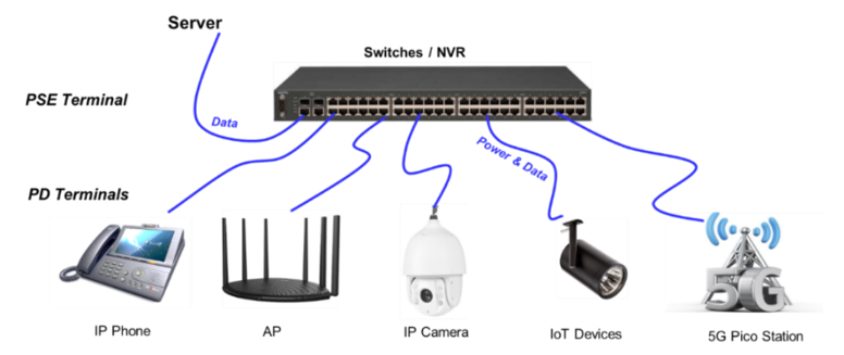
Power over Ethernet (PoE) solutions enable Ethernet cables to transmit DC power while simultaneously transmitting data in parallel to IP terminal devices — all without changing the existing wire connections set by the Ethernet standard. Transmitting power and data in one cable simplifies installation, enhances reliability, and reduces cost by eliminating the need for a power and Ethernet line, which makes PoE devices a popular choice for equipment rooms and offices, as well as older buildings where it may be inconvenient to install new power lines.
This article will provide an overview of PoE PD design, discuss challenges faced by designers implementing these systems, and describe how to optimize a PoE PD design using the MP8017 — an integrated PoE PD and flyback power converter — to verify the recommendations.
PoE Evolution
In 1999, the IEEE and Ethernet Alliance endeavored to standardize PoE, with the goal of ensuring interoperability across a broader range of connected powered devices (PDs) and power sourcing equipment (PSE). The first of these standards, IEEE 802.3af, was ratified in 2003. This standard specified that the power must be able to be carried by either spare pairs or data pairs within a single cable. Today’s PoE standard is the IEEE802.3bt (90W), which covers additional applications such as 5G small cells, display units, and AP routers. Figure 1 shows a timeline of the IEEE PoE standards, beginning with the ≤10W standard in 1999.
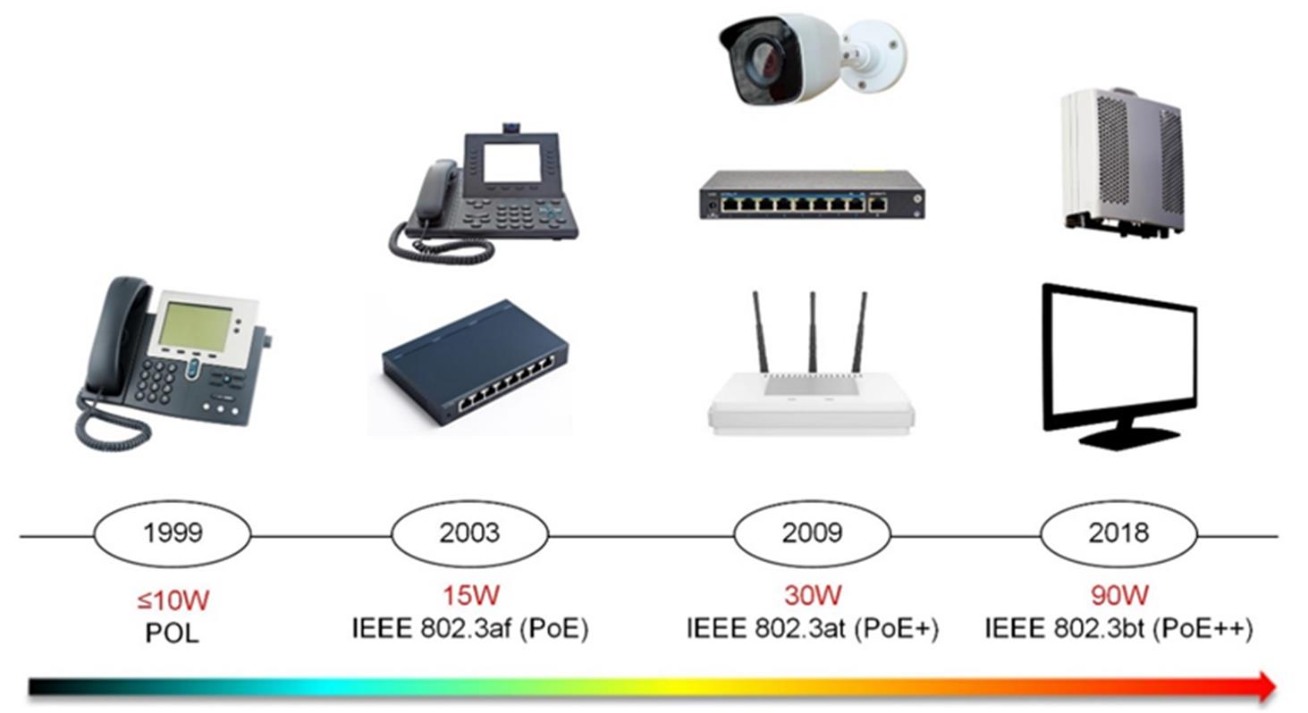
Figure 1: PoE Standard Evolution History
PoE Power Classification
PoE devices are assigned a class (Class 0 through 8, for a total of nine classes) based on the power they require. The 802.3af standard covered Class 0 to Class 3, with voltages ranging between 37V and 57V, and output power up to 15.4. These devices are recommended for sensors and simple cameras.
The 802.3at standard (also known as PoE+) introduced Class 4, which raises the output power to 30W across the same voltage range, though these devices are only compatible with PoE+ PSE. These devices can be used in complex cameras, LCD displays, and tablets.
Lastly, the 802.3bt standard (also called PoE++) introduced Class 5 through Class 8, with output power between 45W and 90W. These devices can support laptops, TVs, and electrical systems in buildings. Figure 2 summarizes these power classes and their related input voltages, input powers, and output voltages.
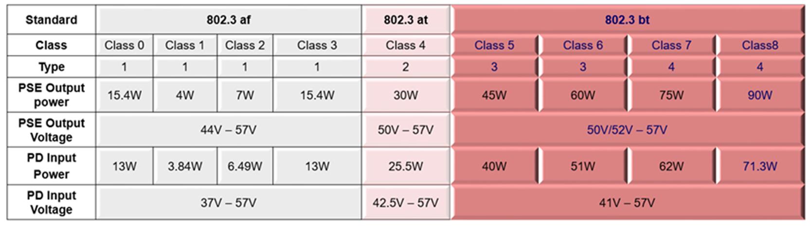
Figure 2: PoE Power Classification
Related Content
-
VIDEO

Understanding Power over Ethernet and PoE Controllers and Converters
Explore what Power over Ethernet (PoE) means for your design
-
ARTICLE
Introducing the MP8017: An Ultra-Small IEEE 802.3af PoE PD Solution
Learn more about our powered device (PD) solutions
-
ARTICLE

Designing a Power over Ethernet (PoE) Solution
Discover the general requirements of PoE and the design of the DC/DC transformation of the PD
-
CATEGORY PAGE
Power Over Ethernet (PoE)
MPS’s PoE ICs enable easy design, simple BOM, and high efficiency
PoE Working Principles
Network cables consist of wires twisted in pairs, with data pairs that are able to send information, and unused pairs that are called spare pairs. When a PD and PSE successfully communicate, it is called a handshake. When the PSE shakes hands with a PD, it follows the main steps listed below:
- PD check: The PSE sends a test voltage (<10.1V) to the PD resistor (24.9kΩ). If the impedance values match, this indicates the presence of a standard PoE device.
- Power classification: The PSE sends one voltage and obtains current feedback to confirm the PD’s power level (from Class 1 to Class 8).
- Supply power: The PSE’s input power rises to about 54V.
- Stabilize power and monitor: The power stabilizes at about 54V, and the maximum power is limited based on the classification results.
- Disconnect: If the PD is disconnected, the PSE stops supplying power.
Figure 3 shows the overall communication structure.
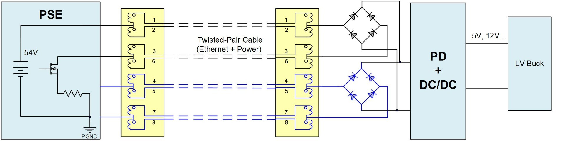
Figure 3: PSE and PD Communication Hardware Structure
Figure 4 shows how voltage levels change while hand shaking occurs between the PSE and PD.
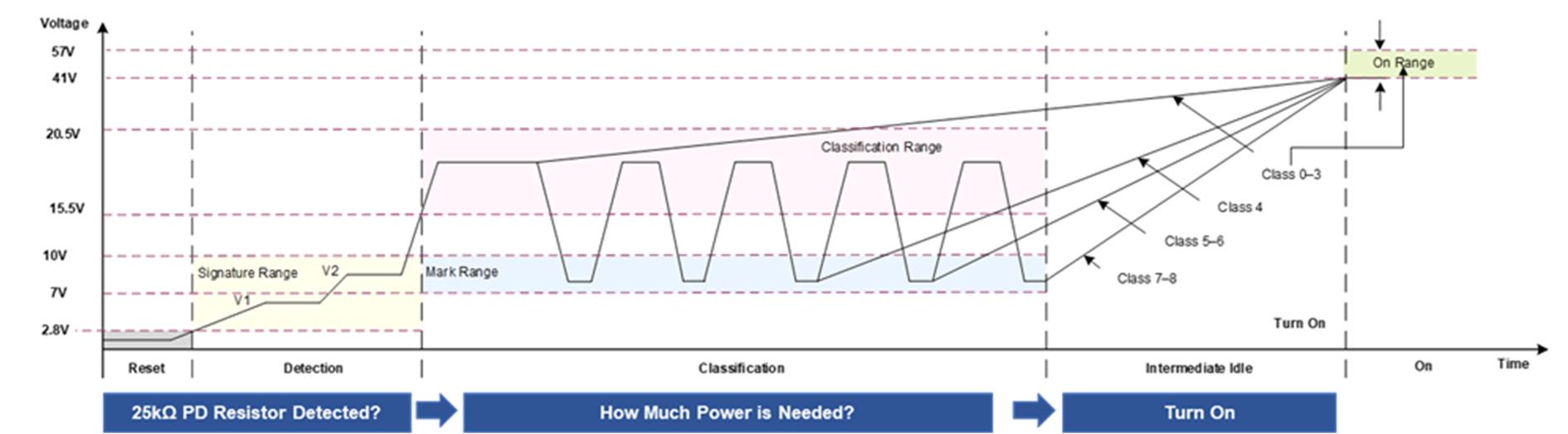
Figure 4: Input Voltage Changes during Handshaking
Challenges when Designing PoE Solutions
PoE devices face a few challenges, the first being efficiency. Although PoE devices incorporate both power and data transfer, they can have lower efficiency if they are not designed correctly. In particular, designers must optimize the power circuit to reduce components’ impedances and select an optimal transformer to improve efficiency.
In addition, the high amount of power transfer creates audible noise, which can affect a device’s ability to meet modern EMI standards. When unregulated, EMI can degrade devices in the surrounding area and reduce a system’s lifetime. PoE devices that supply more power are physically larger, which can take vital room in space-constrained applications.
Figure 5 shows a typical 15W PoE PD power circuit. Due to the number of required components, this circuit is complex and bulky. The optocoupler and TL431 voltage regulator alone comprise their own circuit system with numerous components.
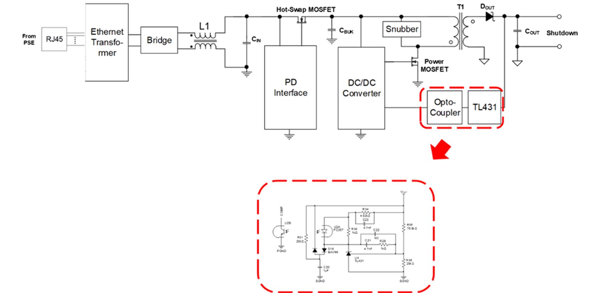
Figure 5: Traditional 15W PD Power Circuit with Optocoupler Feedback
Optimizing a PoE Solution
There are six simple methods to optimize this circuit (see Figure 6).
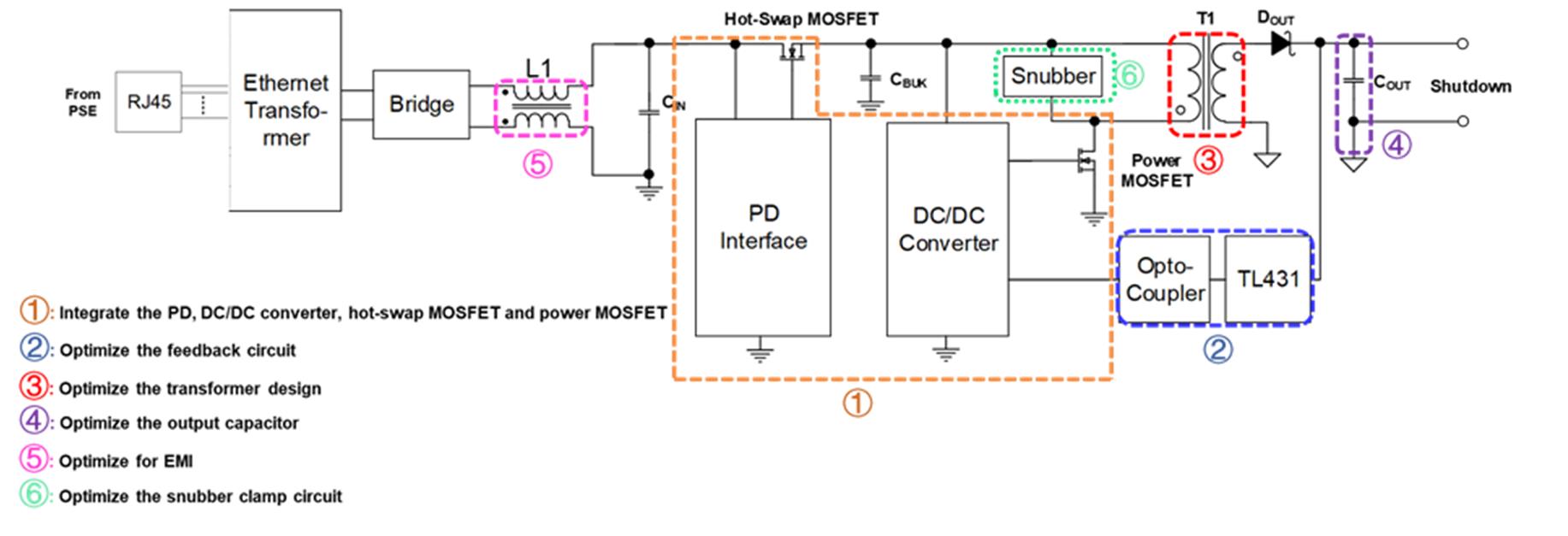
Figure 6: Optimizing a PoE PD Design
These methods are described in greater detail below.
- Full integration: For PoE devices, a completely integrated solution is an excellent way to keep a solution compact. Common questions for PoE solutions include “Can this system include a PD and a DC/DC converter?” and “Can the solution include a hot-swap MOSFET and power MOSFET?”
The answer to both questions is yes. By integrating the PD, converter, and MOSFETs, designers can significantly reduce the PCB size and design cycle. Integrated solutions also reduce the BOM cost, since a simplified solution requires fewer external components. - Feedback circuit: A traditional flyback circuit requires a voltage regulator, optocoupler feedback network, loop compensation, and soft-start circuit. Figure 8 shows the complexity of different circuits, such as a traditional SSR feedback circuit. With the evolution of flyback technology, a primary feedback method was introduced (Gen 1 PSR feedback). This type of circuit typically includes auxiliary winding.
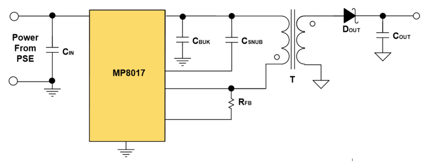
The MP8017 PoE PD solution uses a new feedback method, called Gen 2 PSR feedback. This system does not require auxiliary winding or an optocoupler (see Figure 7). Instead, the device samples the output voltage (VOUT) from the SW pin. Benefits of this method include: - Simplified design circuit since the transformer does not require auxiliary winding
- Reduced transformer cost
- Additional power windings that can be wound on the same core to reduce impedance and improve efficiency.
- Transformer design: For most designs, the transformer is the physically largest and most expensive component in the circuit. Traditionally, an EP13 transformer is used for 12W applications. However, by optimizing the feedback circuit and removing the need for auxiliary winding, designers can implement a high switching frequency (fSW) to reduce the transformer turns. This means an EP7 transformer can replace the EP13, with the EP7 taking up less than a third of the space (see Figure 8).
- Output capacitance: A conventional PoE device has a typical frequency of about 250kHz, and requires electrolytic capacitors to reduce the output ripple. If fSW increases, the number of output capacitors can be reduced. For example, when fSW is 650kHz, a 12W application only needs two ceramic capacitors with a 0805 size. In addition, by utilizing continuous conduction mode (CCM) control, the transformer’s secondary side peak current is smaller. A smaller peak current further reduces the output ripple caused by the output capacitor’s ESR and the layout board’s resistance. Figure 9 compares the secondary current in both CCM and discontinuous conduction mode (DCM).
- EMI design: All relevant devices must pass EMC standards, but it can be challenging to optimize devices for EMI performance. Flyback solutions typically require a common-mode (CM) inductor to improve EMI performance, though this inductor can be expensive and take up vital PCB space. There are two methods to address EMI challenges without using a CM inductor: supporting spread spectrum frequency dithering, and creating smoother SW waveforms. In spread spectrum frequency dithering, fSW fluctuates within its nominal range. The MP8017 supports a dither function using its M/D pin. Its frequency dithering is fixed at ±6%, with a modulation frequency of about 9kHz. Figure 10 shows how using frequency dithering can reduce noise spikes.
- Active snubber: In flyback applications, a resistor capacitor diode (RCD) snubber is widely used as the clamping circuit to reduce SW’s peak voltage and absorb leakage inductance energy. However, this circuit has two issues:
- SW produces resonance, which negatively impacts EMI performance.
- System efficiency is reduced after the leakage inductance energy is consumed.
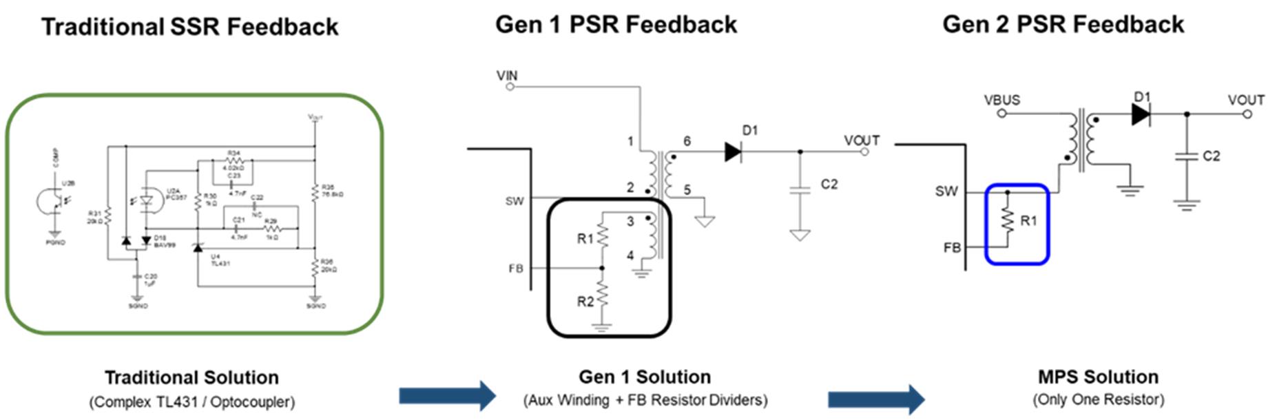
Figure 7: Feedback Solutions Comparison
Using this advanced feedback method simplified the circuit and reduces the BOM.
Figure 8: EP13 Transformer vs. EP7 Transformer
Figure 9: Transformer Secondary Side’s Current in DCM and CCM
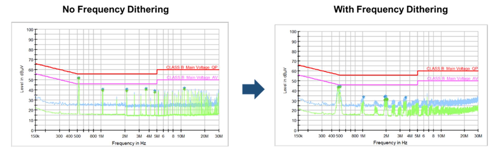
Figure 10: No Frequency Dithering vs. Frequency Dithering
Optimizing the SW waveform is another way to improve EMI (see Figure 11).
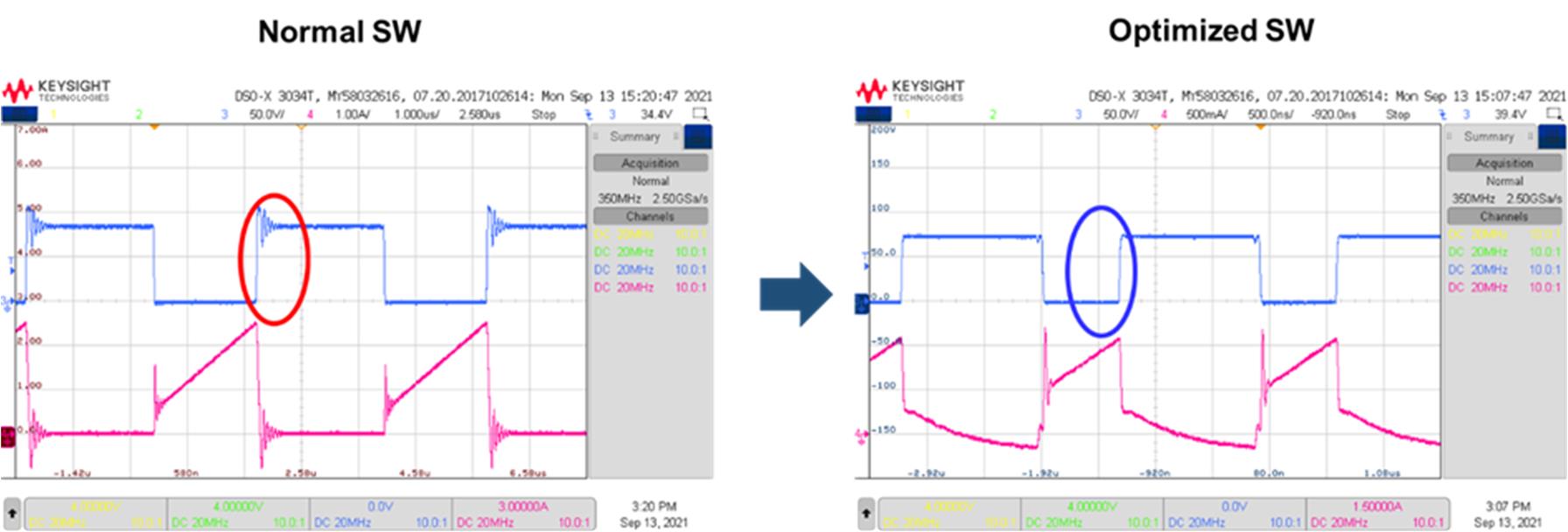
Figure 11: Normal SW vs. Optimized SW
EMI performance was greatly improved after implementing these methods with the MP8017, and the CM inductor was removed without reducing EMI performance.
An active clamp control method can mitigate these issues (see Figure 12). This method uses a power MOSFET to replace the resistor and diode found in a traditional RCD snubber. This allows devices such as the MP8017 to implement secondary-side regulation (SSR), which improves efficiency.
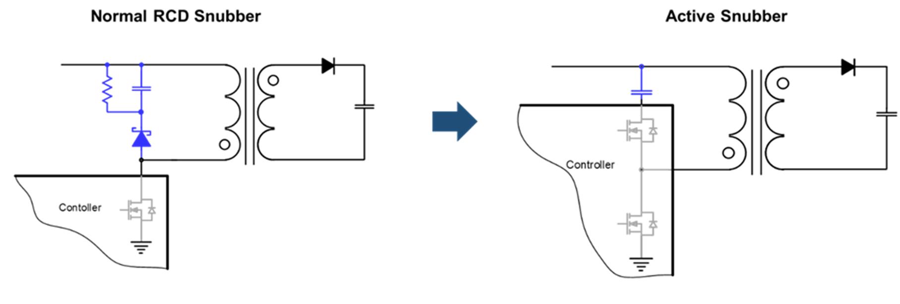
Figure 12: RCD Snubber vs. Active Snubber
By implementing the six main methods listed above, the final circuit can be greatly simplified compared to a traditional circuit (see Figure 13).
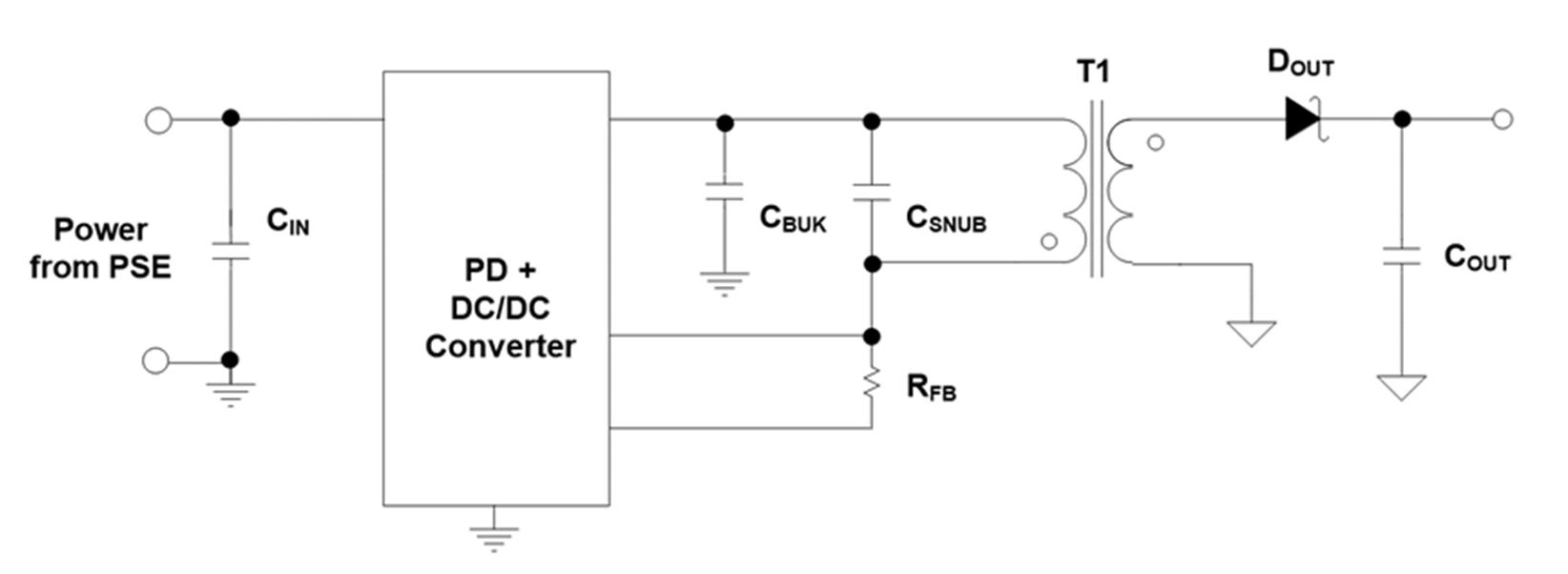
Figure 13: Final Circuit
Conclusion
PoE is an innovative concept that continuously rises to meet the growing power demands of modern technology. Despite its general reliability, it can be difficult for designers to maintain a high efficiency with these solutions, though implementing a few optimization methods can help mitigate these issues. The MP8017 confirmed that selecting optimal transformers, snubbers, and output capacitors — as well as implementing frequency dithering and integrating components onto a single die — are effective methods to guarantee efficient without hindering performance.
_______________________
Did you find this interesting? Get valuable resources straight to your inbox - sent out once per month!
Technical Forum
 Latest activity 4 hours ago
 1 Comment
Latest activity 6 hours ago
1 Comment
Latest activity 6 hours ago
6 Comments
1 Comment
Latest activity 6 hours ago
1 Comment
Latest activity 6 hours ago
6 Comments
Log in to your account
Create New Account