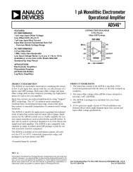
AD548 Precision, Low Power BiFET Op Amp - QRZ.ru
AD548 Precision, Low Power BiFET Op Amp - QRZ.ru
AD548 Precision, Low Power BiFET Op Amp - QRZ.ru

You also want an ePaper? Increase the reach of your titles
YUMPU automatically turns print PDFs into web optimized ePapers that Google loves.
a<br />
FEATURES<br />
Enhanced Replacement for LF441 and TL061<br />
DC Performance:<br />
200 A max Quiescent Current<br />
10 pA max Bias Current, Warmed Up (<strong>AD548</strong>C)<br />
250 V max Offset Voltage (<strong>AD548</strong>C)<br />
2 V/C max Drift (<strong>AD548</strong>C)<br />
2 V p-p Noise, 0.1 Hz to 10 Hz<br />
AC Performance:<br />
1.8 V/s Slew Rate<br />
1 MHz Unity Gain Bandwidth<br />
Available in Plastic, Hermetic Cerdip and Hermetic<br />
Metal Can Packages and in Chip Form<br />
Available in Tape and Reel in Accordance with<br />
EIA-481A Standard<br />
MIL-STD-883B Parts Available<br />
Dual Version Available: AD648<br />
Surface Mount (SOIC) Package Available<br />
PRODUCT DESCRIPTION<br />
The <strong>AD548</strong> is a low power, precision monolithic operational<br />
amplifier. It offers both low bias current (10 pA max, warmed<br />
up) and low quiescent current (200 µA max) and is fabricated<br />
with ion-implanted FET and laser wafer trimming technologies.<br />
Input bias current is guaranteed over the <strong>AD548</strong>’s entire<br />
common-mode voltage range.<br />
The economical J grade has a maximum guaranteed input offset<br />
voltage of less than 2 mV and an input offset voltage drift of less<br />
than 20 µV/°C. The C grade reduces input offset voltage to less<br />
than 0.25 mV and offset voltage drift to less than 2 µV/°C. This<br />
level of dc precision is achieved utilizing Analog’s laser wafer<br />
drift trimming process. The combination of low quiescent current<br />
and low offset voltage drift minimizes changes in input offset<br />
voltage due to self-heating effects. Four additional grades are<br />
offered over the commercial, industrial and military temperature<br />
ranges.<br />
The <strong>AD548</strong> is recommended for any dual supply op amp application<br />
requiring low power and excellent dc and ac performance.<br />
In applications such as battery-powered, precision<br />
inst<strong>ru</strong>ment front ends and CMOS DAC buffers, the <strong>AD548</strong>’s<br />
excellent combination of low input offset voltage and drift, low<br />
bias current and low 1/f noise reduces output errors. High common-mode<br />
rejection (86 dB, min on the “C” grade) and high<br />
open-loop gain ensures better than 12-bit linearity in high impedance,<br />
buffer applications.<br />
The <strong>AD548</strong> is pinned out in a standard op amp configuration<br />
and is available in six performance grades. The <strong>AD548</strong>J and<br />
<strong>AD548</strong>K are rated over the commercial temperature range of<br />
0°C to +70°C. The <strong>AD548</strong>A, <strong>AD548</strong>B and <strong>AD548</strong>C are rated<br />
OFFSET NULL<br />
1<br />
INVERTING<br />
INPUT<br />
2<br />
3<br />
NONINVERTING<br />
INPUT<br />
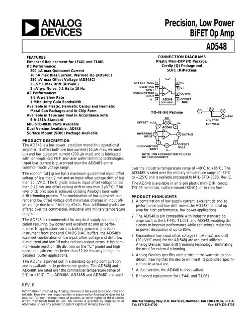
<strong>Precision</strong>, <strong>Low</strong> <strong>Power</strong><br />
<strong>BiFET</strong> <strong>Op</strong> <strong>Amp</strong><br />
<strong>AD548</strong><br />
CONNECTION DIAGRAMS<br />
Plastic Mini-DIP (N) Package,<br />
Cerdip (Q) Package and<br />
SOIC (R)Package<br />
OFFSET NULL 1<br />
8 NC<br />
INVERTING<br />
INPUT<br />
NONINVERTING<br />
INPUT<br />
V–<br />
2<br />
3<br />
4 <strong>AD548</strong><br />
TOP VIEW<br />
7<br />
6<br />
5<br />
V+<br />
OUTPUT<br />
OFFSET<br />
NULL<br />
TO-99 (H) Package<br />
NC<br />
8 V+<br />
<strong>AD548</strong> 7<br />
4<br />
V–<br />
5<br />
6<br />
OUTPUT<br />
OFFSET<br />
NULL<br />
NOTE : PIN 4 CONNECTED TO CASE<br />
NC = NO CONNECT<br />
over the industrial temperature range of –40°C to +85°C. The<br />
<strong>AD548</strong>S is rated over the military temperature range of –55°C<br />
to +125°C and is available processed to MIL-STD-883B, Rev. C.<br />
The <strong>AD548</strong> is available in an 8-pin plastic mini-DIP, cerdip,<br />
TO-99 metal can, surface mount (SOIC), or in chip form.<br />
PRODUCT HIGHLIGHTS<br />
1. A combination of low supply current, excellent dc and ac<br />
performance and low drift makes the <strong>AD548</strong> the ideal op<br />
amp for high performance, low power applications.<br />
2. The <strong>AD548</strong> is pin compatible with industry standard op<br />
amps such as the LF441, TL061, and AD542, enabling designers<br />
to improve performance while achieving a reduction<br />
in power dissipation of up to 85%.<br />
3. Guaranteed low input offset voltage (2 mV max) and drift<br />
(20 µV/°C max) for the <strong>AD548</strong>J are achieved utilizing<br />
Analog Devices’ laser drift trimming technology, eliminating<br />
the need for external trimming.<br />
4. Analog Devices specifies each device in the warmed-up condition,<br />
insuring that the device will meet its published specifications<br />
in actual use.<br />
5. A dual version, the AD648 is also available.<br />
6. Enhanced replacement for LF441 and TL061.<br />
1<br />
10kΩ<br />
V OS TRIM<br />
TOP VIEW<br />
5<br />
4<br />
–15V<br />
REV. B<br />
Information furnished by Analog Devices is believed to be accurate and<br />
reliable. However, no responsibility is assumed by Analog Devices for its<br />
use, nor for any infringements of patents or other rights of third parties<br />
which may result from its use. No license is granted by implication or<br />
otherwise under any patent or patent rights of Analog Devices.<br />
One Technology Way, P.O. Box 9106, Norwood, MA 02062-9106, U.S.A.<br />
Tel: 617/329-4700 Fax: 617/326-8703
<strong>AD548</strong>–SPECIFICATIONS<br />
(@ +25C and V S = 15 V dc unless otherwise noted)<br />
Model <strong>AD548</strong>J/A/S <strong>AD548</strong>K/B <strong>AD548</strong>C<br />
Min Typ Max Min Typ Max Min Typ Max Units<br />
INPUT OFFSET VOLTAGE 1<br />
Initial Offset 0.75 2.0 0.3 0.5 0.10 0.25 mV<br />
T MIN to T MAX 3.0/3.0/3.0 0.7/0.8 0.4 mV<br />
vs. Temperature 20 5 2.0 µV/°C<br />
vs. Supply 80 86 86 dB<br />
vs. Supply, T MIN to T MAX 76/76/76 80 80 dB<br />
Long-Term Offset Stability 15 15 15 µV/Month<br />
INPUT BIAS CURRENT<br />
Either Input 2 , V CM = 0 5 20 3 10 3 10 pA<br />
Either Input 2 at T MAX , V CM = 0 0.45/1.3/20 0.25/0.65 0.65 nA<br />
Max Input Bias Current Over<br />
Common-Mode Voltage Range 30 15 15 pA<br />
Offset Current, V CM = 0 5 10 2 5 2 5 pA<br />
Offset Current at T MAX 0.25/0.65/10 0.15/0.35 0.35 nA<br />
INPUT IMPEDANCE<br />
Differential 1 × 10 12 3 1 × 10 12 3 1 × 10 12 3 ΩpF<br />
Common Mode 3 × 10 12 3 3 × 10 12 3 3 × 10 12 3 ΩpF<br />
INPUT VOLTAGE RANGE<br />
Differential 3 ±20 ±20 ±20 V<br />
Common Mode ±11 ±12 ±11 ±12 ±11 ±12 V<br />
Common-Mode Rejection<br />
V CM = ±10 V 76 90 82 92 86 98 dB<br />
T MIN to T MAX 76/76/76 90 82 92 86 98 dB<br />
V CM = ±11 V 70 84 76 86 76 90 dB<br />
T MIN to T MAX 70/70/70 84 76 86 76 90 dB<br />
INPUT VOLTAGE NOISE<br />
Voltage 0.1 Hz to 10 Hz 2 2 2 4.0 µV p-p<br />
f = 10 Hz 80 80 80 nV/√Hz<br />
f = 100 Hz 40 40 40 nV/√Hz<br />
f = 1 kHz 30 30 30 nV/√Hz<br />
f = 10 kHz 30 30 30 nV/√Hz<br />
INPUT CURRENT NOISE<br />
f = 1 kHz 1.8 1.8 1.8 fA/√Hz<br />
FREQUENCY RESPONSE<br />
Unity Gain, Small Signal 0.8 1.0 0.8 1.0 0.8 1.0 MHz<br />
Full <strong>Power</strong> Response 30 30 30 kHz<br />
Slew Rate, Unity Gain 1.0 1.8 1.0 1.8 1.0 1.8 V/µs<br />
Settling Time to ± 0.01% 8 8 8 µs<br />
OPEN LOOP GAIN<br />
V O = ± 10 V, R L ≥ 10 kΩ 300 1000 300 1000 300 1000 V/mV<br />
T MIN to T MAX , R L ≥ 10 kΩ 300/300/300 700 300 700 300 700 V/mV<br />
V O = ± 10 V, R L ≥ 5 kΩ 150 500 150 500 150 500 V/mV<br />
T MIN to T MAX , R L ≥ 5 kΩ 150/150/150 300 150 300 150 300 V/mV<br />
OUTPUT CHARACTERISTICS<br />
Voltage @ R L ≥ 10 kΩ, ±12 ±13 ±12 ±13 ±12 ±13 V<br />
T MIN to T MAX ±12/± 12/± 12 ±12 ±12<br />
Voltage @ R L ≥ 5 kΩ, ±11 ±12.3 ±11 ±12.3 ±11 ±12.3 V<br />
T MIN to T MAX ±11/± 11/± 11 ±11 ±11<br />
Short Circuit Current 15 15 15 mA<br />
POWER SUPPLY<br />
Rated Performance ±15 ±15 ±15 V<br />
<strong>Op</strong>erating Range ±4.5 ±18 ±4.5 ±18 ±4.5 ±18 V<br />
Quiescent Current 170 200 170 200 170 200 µA<br />
TEMPERATURE RANGE<br />
<strong>Op</strong>erating, Rated Performance<br />
Commercial (0°C to +70°C) <strong>AD548</strong>J <strong>AD548</strong>K<br />
Industrial (–40°C to +85°C) <strong>AD548</strong>A <strong>AD548</strong>B <strong>AD548</strong>C<br />
Military (–55°C to +125°C)<br />
<strong>AD548</strong>S<br />
PACKAGE OPTIONS<br />
SOIC (R-8) <strong>AD548</strong>JR <strong>AD548</strong>KR, <strong>AD548</strong>BR<br />
Plastic (N-8) <strong>AD548</strong>JN <strong>AD548</strong>KN<br />
Cerdip (Q-8) <strong>AD548</strong>AQ <strong>AD548</strong>CQ<br />
Metal Can (H-08A) <strong>AD548</strong>AH <strong>AD548</strong>BH<br />
Tape and Reel <strong>AD548</strong>JR-REEL <strong>AD548</strong>KR-REEL, <strong>AD548</strong>BR-REEL<br />
Chips Available <strong>AD548</strong>JCHIPS<br />
NOTES<br />
1 Input Offset Voltage specifications are guaranteed after 5 minutes of operation at TA = +25°C.<br />
2 Bias Current specifications are guaranteed maximum at either input after 5 minutes of operation at T A = +25°C. For higher temperature, the current doubles every 10°C.<br />
3 Defined as voltages between inputs, such that neither exceeds ±10 V from ground.<br />
Specifications subject to change without notice.<br />
–2–<br />
REV. C
<strong>AD548</strong><br />
ABSOLUTE MAXIMUM RATINGS l<br />
Supply Voltage . . . . . . . . . . . . . . . . . . . . . . . . . . . . . . . . .±18 V<br />
Internal <strong>Power</strong> Dissipation 2 . . . . . . . . . . . . . . . . . . . . 500 mW<br />
Input Voltage 3 . . . . . . . . . . . . . . . . . . . . . . . . . . . . . . . . .±18 V<br />
Output Short Circuit Duration . . . . . . . . . . . . . . . . .Indefinite<br />
Differential Input Voltage . . . . . . . . . . . . . . . . . . +V S and –V S<br />
Storage Temperature Range (Q, H) . . . . . . . . –65°C to +150°C<br />
(N, R) . . . . . . . . –65°C to +125°C<br />
<strong>Op</strong>erating Temperature Range<br />
<strong>AD548</strong>J/K . . . . . . . . . . . . . . . . . . . . . . . . . . . .0°C to +70°C<br />
<strong>AD548</strong>A/B/C . . . . . . . . . . . . . . . . . . . . . . . . –40°C to +85°C<br />
<strong>AD548</strong>S . . . . . . . . . . . . . . . . . . . . . . . . . . . –55°C to +125°C<br />
Lead Temperature Range (Soldering 60 sec) . . . . . . . . +300°C<br />
NOTES<br />
1 Stresses above those listed under “Absolute Maximum Ratings” may cause<br />
permanent damage to the device. This is a stress rating only and functional<br />
operation of the device at these or any other conditions above those indicated in the<br />
operational sections of this specification is not implied. Exposure to absolute<br />
maximum rating conditions for extended periods may affect device reliability.<br />
2 Thermal Characteristics: 8-Pin SOIC Package: θ JA = 160°C/W, θ JC = 42°C/W;<br />
8-Pin Plastic Package: θ JA = 90°C/W; 8-Pin Cerdip Package: θ JC = 22°C/W, θ JA =<br />
110°C/W; 8-Pin Metal Can Package: θ JC = 65°C/W, θ JA = 150°C/W.<br />
3 For supply voltages less than ±18 V, the absolute maximum input voltage is equal<br />
to the supply voltage.<br />
20<br />
20<br />
METALIZATION PHOTOGRAPH<br />
Dimensions shown in inches and (mm).<br />
Contact factory for latest dimensions<br />
30<br />
Typical Characteristics<br />
INPUT VOLTAGE – ±V<br />
15<br />
10<br />
5<br />
+V IN<br />
–V IN<br />
OUTPUT VOLTAGE SWING – ±V<br />
15<br />
10<br />
5<br />
+V OUT<br />
–V OUT<br />
25°C<br />
R L = 10k<br />
OUTPUT VOLTAGE SWING – Volts p-p<br />
25<br />
20<br />
15<br />
10<br />
5<br />
0<br />
0 5 10 15 20<br />
SUPPLY VOLTAGE – ±V<br />
Figure 1. Input Voltage Range<br />
vs. Supply Voltage<br />
0<br />
0 5 10 15 20<br />
SUPPLY VOLTAGE – ±V<br />
Figure 2. Output Voltage Swing<br />
vs. Supply Voltage<br />
0<br />
10 100 1k 10k<br />
LOAD RESISTANCE – Ω<br />
Figure 3. Output Voltage Swing<br />
vs. Load Resistance<br />
200<br />
10<br />
100nA<br />
QUIESCENT CURRENT – µA<br />
180<br />
160<br />
140<br />
INPUT BIAS CURRENT – pA<br />
8<br />
6<br />
4<br />
2<br />
INPUT BIAS CURRENT<br />
10nA<br />
1nA<br />
100pA<br />
10pA<br />
1pA<br />
100fA<br />
120<br />
0 5 10 15 20<br />
SUPPLY VOLTAGE – ±V<br />
Figure 4. Quiescent Current vs.<br />
Supply Voltage<br />
0<br />
0 4 8 12 16 20<br />
SUPPLY VOLTAGE – ±V<br />
Figure 5. Input Bias Current<br />
vs. Supply Voltage<br />
10fA<br />
–55 –25 5 35 65 95 125<br />
TEMPERATURE – °C<br />
Figure 6. Input Bias Current vs.<br />
Temperature<br />
CAUTION<br />
ESD (electrostatic discharge) sensitive device. Electrostatic charges as high as 4000 V readily<br />
accumulate on the human body and test equipment and can discharge without detection.<br />
Although the <strong>AD548</strong> features proprietary ESD protection circuitry, permanent damage may<br />
occur on devices subjected to high energy electrostatic discharges. Therefore, proper ESD<br />
precautions are recommended to avoid performance degradation or loss of functionality.<br />
WARNING!<br />
ESD SENSITIVE DEVICE<br />
REV. C –3–
<strong>AD548</strong>–Typical Characteristics<br />
INPUT BIAS CURRENT – pA<br />
10<br />
8<br />
6<br />
4<br />
2<br />
I∆V OS I – µV<br />
30<br />
25<br />
20<br />
15<br />
10<br />
5<br />
OPEN LOOP GAIN – V/mV<br />
1500<br />
1250<br />
1000<br />
750<br />
500<br />
250<br />
R L = 10k<br />
0<br />
–10 –6 –2 2 6 10<br />
COMMON-MODE VOLTAGE – V<br />
Figure 7. Input Bias Current vs.<br />
Common-Mode Voltage<br />
0 0 10 20 30 40 50 60 70<br />
WARM-UP TIME – Seconds<br />
Figure 8. Change in Offset Voltage<br />
vs. Warm-Up Time<br />
0<br />
–55 –25 5 35 65 95 125<br />
TEMPERATURE – °C<br />
Figure 9. <strong>Op</strong>en Loop Gain vs.<br />
Temperature<br />
100<br />
100<br />
120<br />
120<br />
OPEN LOOP GAIN – dB<br />
80<br />
60<br />
40<br />
20<br />
0<br />
–20<br />
PHASE<br />
GAIN<br />
80<br />
60<br />
40<br />
20<br />
0<br />
–20<br />
PHASE IN DEGREES<br />
OPEN LOOP VOLTAGE GAIN – dB<br />
110<br />
100<br />
90<br />
80<br />
70<br />
POWER SUPPLY REJECTION – dB<br />
100<br />
80<br />
60<br />
40<br />
20<br />
0<br />
+SUPPLY<br />
–SUPPLY<br />
–40 –40<br />
1k 10k 100k 1M 10M<br />
FREQUENCY – Hz<br />
Figure 10. <strong>Op</strong>en Loop Frequency<br />
Response<br />
CMRR – dB<br />
TOTAL HARMONIC DISTORTION – %<br />
90<br />
80<br />
70<br />
60<br />
50<br />
40<br />
30<br />
20<br />
1k 10k 100k 1M<br />
FREQUENCY – Hz<br />
Figure 13. CMRR vs. Frequency<br />
4<br />
1<br />
0.1<br />
0.01<br />
FOLLOWER<br />
WITH GAIN = 10<br />
UNITY GAIN<br />
FOLLOWER<br />
0.001<br />
100 1k 10k<br />
FREQUENCY – Hz<br />
Figure 16. Total Harmonic<br />
Distortion vs. Frequency<br />
100k<br />
60<br />
0 2 4 6 8 10 12 14 16 18<br />
SUPPLY VOLTAGE – ±V<br />
Figure 11. <strong>Op</strong>en Loop Voltage Gain<br />
vs. Supply Voltage<br />
OUTPUT VOLTAGE – V p-p<br />
22<br />
20<br />
18<br />
16<br />
14<br />
12<br />
10<br />
8<br />
6<br />
4<br />
2<br />
0<br />
10 100 1k 10k 100k 1M<br />
FREQUENCY – Hz<br />
Figure 14. Large Signal Frequency<br />
Response<br />
INPUT NOISE VOLTAGE – nV/√Hz<br />
160<br />
140<br />
120<br />
100<br />
80<br />
60<br />
40<br />
20<br />
0<br />
10 100 1k 10k 100k<br />
FREQUENCY – Hz<br />
Figure 17. Input Noise Voltage<br />
Spectral Density<br />
OUTPUT VOLTAGE SWING – V<br />
–20<br />
100 1k 10k 100k 1M<br />
FREQUENCY – Hz<br />
Figure 12. PSRR vs. Frequency<br />
10<br />
5<br />
0<br />
–5<br />
10mV<br />
1mV<br />
1mV<br />
10mV<br />
–10<br />
0 2 4 6 8<br />
SETTLING TIME – µs<br />
Figure 15. Output Swing and Error<br />
Voltage vs. Output Settling Time<br />
INPUT NOISE VOLTAGE – µV p-p<br />
10,000<br />
1,000<br />
100<br />
10<br />
WHENEVER JOHNSON NOISE IS GREATER THAN<br />
AMPLIFIER NOISE, AMPLIFIER NOISE CAN BE<br />
CONSIDERED NEGLIGIBLE FOR APPLICATION<br />
1kHz BANDWIDTH<br />
RESISTOR JOHNSON<br />
NOISE<br />
10Hz<br />
BANDWIDTH<br />
1<br />
AMPLIFIER GENERATED NOISE<br />
0<br />
100k 1M 10M 100M 1G 10G 100G<br />
SOURCE IMPEDANCE – Ω<br />
Figure 18. Total Noise vs. Source<br />
Impedance<br />
–4– REV. C
Typical Characteristics–<strong>AD548</strong><br />
Figure 19a. Unity Gain Follower<br />
Figure 19b. Unity Gain Follower<br />
Pulse Response (Large Signal)<br />
Figure 19c. Unity Gain Follower<br />
Pulse Response (Small Signal)<br />
Figure 20a. Utility Gain Inverter<br />
APPLICATION NOTES<br />
The <strong>AD548</strong> is a JFET-input op amp with a guaranteed maximum<br />
I B of less than 10 pA, and offset and drift laser-trimmed to<br />
0.25 mV and 2 µV/°C respectively (<strong>AD548</strong>C). AC specs include<br />
1 MHz bandwidth, 1.8 V/µs typical slew rate and 8 µs settling<br />
time for a 20 V step to ±0.01%—all at a supply current less<br />
than 200 µA. To capitalize on the device’s performance, a number<br />
of error sources should be considered.<br />
The minimal power drain and low offset drift of the <strong>AD548</strong><br />
reduce self-heating or “warm-up” effects on input offset voltage,<br />
making the <strong>AD548</strong> ideal for on/off battery powered applications.<br />
The power dissipation due to the <strong>AD548</strong>’s 200 µA supply<br />
current has a negligible effect on input current, but heavy output<br />
loading will raise the chip temperature. Since a JFET’s input<br />
current doubles for every 10°C rise in chip temperature, this<br />
can be a noticeable effect.<br />
The amplifier is designed to be functional with power supply<br />
voltages as low as ±4.5 V. It will exhibit a higher input offset<br />
voltage than at the rated supply voltage of ±15 V, due to power<br />
supply rejection effects. The common-mode range of the<br />
<strong>AD548</strong> extends from 3 V more positive than the negative supply<br />
to 1 V more negative than the positive supply. Designed to<br />
cleanly drive up to 10 kΩ and 100 pF loads, the <strong>AD548</strong> will<br />
drive a 2 kΩ load with reduced open loop gain.<br />
OFFSET NULLING<br />
Unlike bipolar input amplifiers, zeroing the input offset voltage<br />
of a <strong>BiFET</strong> op amp will not minimize offset drift. Using balance<br />
Pins 1 and 5 to adjust the input offset voltage as shown in Figure<br />
21 will induce an added drift of 0.24 µV/°C per 100 µV of<br />
nulled offset. The low initial offset (0.25 mV) of the <strong>AD548</strong>C<br />
results in only 0.6 µV/°C of additional drift.<br />
Figure 20b. Utility Gain Inverter<br />
Pulse Response (Large Signal)<br />
Applying the <strong>AD548</strong><br />
Figure 20c. Unity Gain Inverter<br />
Pulse Response (Small Signal)<br />
Figure 21. Offset Null Configuration<br />
LAYOUT<br />
To take full advantage of the <strong>AD548</strong>’s 10 pA max input current,<br />
parasitic leakages must be kept below an acceptable level. The<br />
practical limit of the resistance of epoxy or phenolic circuit<br />
board material is between 1 × 10 12 Ω and 3 × 10 12 Ω. This can<br />
result in an additional leakage of 5 pA between an input of 0 V<br />
and a –15 V supply line. Teflon or a similar low leakage material<br />
(with a resistance exceeding 10 17 Ω) should be used to isolate<br />
high impedance input lines from adjacent lines carrying high<br />
voltages. The insulator should be kept clean, since contaminants<br />
will degrade the surface resistance.<br />
A metal guard completely surrounding the high impedance<br />
nodes and driven by a voltage near the common-mode input potential<br />
can also be used to reduce some parasitic leakages. The<br />
guarding pattern in Figure 22 will reduce parasitic leakage due<br />
to finite board surface resistance; but it will not compensate for<br />
a low volume resistivity board.<br />
REV. C –5–
<strong>AD548</strong><br />
Figure 22. Board Layout for Guarding Inputs<br />
INPUT PROTECTION<br />
The <strong>AD548</strong> is guaranteed to withstand input voltages equal to<br />
the power supply potential. Exceeding the negative supply voltage<br />
on either input will forward bias the substrate junction of<br />
the chip. The induced current may destroy the amplifier due to<br />
excess heat.<br />
Input protection is required in applications such as a flame<br />
detector in a gas chromatograph, where a very high potential<br />
may be applied to the input terminals during a sensor fault condition.<br />
Figure 23 shows a simple current limiting scheme that<br />
can be used. R PROTECT should be chosen such that the maximum<br />
overload current is 1.0 mA (l00 kΩ for a 100 V overload,<br />
for example).<br />
Exceeding the negative common-mode range on either input<br />
terminal causes a phase reversal at the output, forcing the<br />
amplifier output to the corresponding high or low state. Exceeding<br />
the negative common-mode on both inputs simultaneously<br />
forces the output high. Exceeding the positive common-mode<br />
range on a single input doesn’t cause a phase reversal, but if<br />
both inputs exceed the limit the output will be forced high. In<br />
all cases, normal amplifier operation is resumed when input<br />
voltages are brought back within the common-mode range.<br />
Figure 24. <strong>AD548</strong> Used as DAC Output <strong>Amp</strong>lifier<br />
That is:<br />
⎛<br />
V OS Output =V OS Input 1+ R FB ⎞<br />
⎜<br />
⎝ R<br />
⎟<br />
O ⎠<br />
R FB is the feedback resistor for the op amp, which is internal to<br />
the DAC. R O is the DAC’s R-2R ladder output resistance. The<br />
value of R O is code dependent. This has the effect of changing<br />
the offset error voltage at the amplifier’s output. An output amplifier<br />
with a sub millivolt input offset voltage is needed to<br />
preserve the linearity of the DAC’s transfer function.<br />
The <strong>AD548</strong> in this configuration provides a 700 kHz small signal<br />
bandwidth and 1.8 V/µs typical slew rate. The 33 pF capacitor<br />
across the feedback resistor optimizes the circuit’s response.<br />
The oscilloscope photos in Figures 25 and 26 show small and<br />
large signal outputs of the circuit in Figure 24. Upper traces<br />
show the input signal V IN . <strong>Low</strong>er traces are the resulting output<br />
voltage with the DAC’s digital input set to all 1s. The <strong>AD548</strong><br />
settles to ±0.01% for a 20 V input step in 14 µs.<br />
5V 20V<br />
5µS<br />
100<br />
90<br />
10<br />
0%<br />
Figure 25. Response to ±20 V p-p Reference Square Wave<br />
Figure 23. Input Protection of IV Converter<br />
D/A CONVERTER OUTPUT BUFFER<br />
The circuit in Figure 24 shows the <strong>AD548</strong> and AD7545 12-bit<br />
CMOS D/A converter in a unipolar binary configuration. V OUT<br />
will be equal to V REF attenuated by a factor depending on the<br />
digital word. V REF sets the full scale. Overall gain is trimmed by<br />
adjusting R IN . The <strong>AD548</strong>’s low input offset voltage, low drift<br />
and clean dynamics make it an attractive low power output<br />
buffer.<br />
The input offset voltage of the <strong>AD548</strong> output amplifier results<br />
in an output error voltage. This error voltage equals the input<br />
offset voltage of the op amp times the noise gain of the<br />
amplifier.<br />
100<br />
90<br />
10<br />
0%<br />
50mV 200mV<br />
2µS<br />
Figure 26. Response to ±100 mV p-p Reference Square<br />
Wave<br />
–6– REV. C
Application Hints–<strong>AD548</strong><br />
PHOTODIODE PREAMP<br />
The performance of the photodiode preamp shown in Figure 27<br />
is enhanced by the <strong>AD548</strong>’s low input current, input voltage<br />
offset and offset voltage drift. The photodiode sources a current<br />
proportional to the incident light power on its surface. R F converts<br />
the photodiode current to an output voltage equal to R F × I S .<br />
Figure 27.<br />
An error budget illustrating the importance of low amplifier<br />
input current, voltage offset and offset voltage drift to minimize<br />
output voltage errors can be developed by considering the equivalent<br />
circuit for the small (0.2 mm 2 area) photodiode shown in<br />
Figure 27. The input current results in an error proportional to<br />
the feedback resistance used. The amplifier’s offset will produce<br />
an error proportional to the preamp’s noise gain (I + R F /R SH ),<br />
where R SH is the photodiode shunt resistance. The amplifier’s<br />
input current will double with every 10°C rise in temperature,<br />
and the photodiode’s shunt resistance halves with every 10°C<br />
rise. The error budget in Figure 28 assumes a room temperature<br />
photodiode R SH of 500 MΩ, and the maximum input current<br />
and input offset voltage specs of an <strong>AD548</strong>C.<br />
TEMP<br />
C R SH (M) V OS (V) (1+ R F /R SH ) V OS I B (pA) I B R F TOTAL<br />
–25 15,970 150 151 µV 0.30 30 µV 181 µV<br />
0 2,830 200 207 µV 2.26 262 µV 469 µV<br />
+25 500 250 300 µV 10.00 1.0 mV 1.30 mV<br />
+50 88.5 300 640 µV 56.6 5.6 mV 6.24 mV<br />
+75 15.6 350 2.6 mV 320 32 mV 34.6 mV<br />
+85 7.8 370 5.1 mV 640 64 mV 69.1 mV<br />
Figure 28. Photo Diode Pre-<strong>Amp</strong> Errors Over Temperature<br />
The capacitance at the amplifier’s negative input (the sum of the<br />
photodiode’s shunt capacitance, the op amp’s differential input<br />
capacitance, stray capacitance due to wiring, etc.) will cause a<br />
rise in the preamp’s noise gain over frequency. This can result in<br />
excess noise over the bandwidth of interest. C F reduces the<br />
noise gain “peaking” at the expense of bandwidth.<br />
INSTRUMENTATION AMPLIFIER<br />
The <strong>AD548</strong>C’s maximum input current of 10 pA makes it an<br />
excellent building block for the high input impedance inst<strong>ru</strong>mentation<br />
amplifier shown in Figure 29. Total current drain for<br />
this circuit is under 600 µA. This configuration is optimal for<br />
conditioning differential voltages from high impedance sources.<br />
The overall gain of the circuit is controlled by R G , resulting in<br />
the following transfer function:<br />
V OUT<br />
V IN<br />
= 1 + (R 1 + R 2 )<br />
R G<br />
REV. C –7–<br />
Figure 29. <strong>Low</strong> <strong>Power</strong> Inst<strong>ru</strong>mentation <strong>Amp</strong>lifier<br />
Gains of 1 to 100 can be accommodated with gain nonlinearities<br />
of less than 0.01%. Referred to input errors, which contribute<br />
an output error proportional to in amp gain, include a maximum<br />
untrimmed input offset voltage of 0.5 mV and an input<br />
offset voltage drift over temperature of 4 µV/°C. Output errors,<br />
which are independent of gain, will contribute an additional<br />
0.5 mV offset and 4 µV/°C drift. The maximum input current is<br />
15 pA over the common-mode range, with a common-mode<br />
impedance of over 1 × 10 12 Ω. Resistor pairs R3/R5 and R4/R6<br />
should be ratio matched to 0.01% to take full advantage of the<br />
<strong>AD548</strong>’s high common-mode rejection. Capacitors C1 and C1′<br />
compensate for peaking in the gain over frequency caused by<br />
input capacitance when gains of 1 to 3 are used.<br />
The –3 dB small signal bandwidth for this low power inst<strong>ru</strong>mentation<br />
amplifier is 700 kHz for a gain of 1 and 10 kHz for a<br />
gain of 100. The typical output slew rate is 1.8 V/µs.<br />
LOG RATIO AMPLIFIER<br />
Log ratio amplifiers are useful for a variety of signal conditioning<br />
applications, such as linearizing exponential transducer outputs<br />
and compressing analog signals having a wide dynamic<br />
range. The <strong>AD548</strong>’s picoamp level input current and low input<br />
offset voltage make it a good choice for the front-end amplifier<br />
of the log ratio circuit shown in Figure 30. This circuit produces<br />
an output voltage equal to the log base 10 of the ratio of the input<br />
currents I 1 and I 2 . Resistive inputs R1 and R2 are provided<br />
for voltage inputs.<br />
Input currents I 1 and I 2 set the collector currents of Q1 and Q2,<br />
a matched pair of logging transistors. Voltages at points A and<br />
B are developed according to the following familiar diode<br />
equation:<br />
V BE<br />
= (kT/q)ln(I C<br />
/I ES<br />
)<br />
In this equation, k is Boltzmann’s constant, T is absolute temperature,<br />
q is an electron charge, and I ES is the reverse saturation<br />
current of the logging transistors. The difference of these two<br />
voltages is taken by the subtractor section and scaled by a factor<br />
of approximately 16 by resistors R9, R10, and R8. Temperature
<strong>AD548</strong><br />
OUTLINE DIMENSIONS<br />
Dimensions shown in inches and (mm).<br />
TO-99 (H) Package<br />
Figure 30. Log Ratio <strong>Amp</strong>lifier<br />
compensation is provided by resistors R8 and R15, which have a<br />
positive 3500 ppm/°C temperature coefficient. The transfer<br />
function for the output voltage is:<br />
V OUT = 1V log 10 (I 2 /I 1 )<br />
Frequency compensation is provided by R11, R12, C1, and C2.<br />
Small signal bandwidth is approximately 300 kHz at input currents<br />
above 100 µA and will proportionally decrease with lower<br />
signal levels. D1, D2, R13, and R14 compensate for the effects<br />
of the two logging transistors’ ohmic emitter resistance.<br />
To trim this circuit, set the two input currents to 10 µA and adjust<br />
V OUT to zero by adjusting the potentiometer on A3. Then<br />
set I 2 to 1 µA and adjust the scale factor such that the output<br />
voltage is 1 V by trimming potentiometer R10. Offset adjustment<br />
for A1 and A2 is provided to increase the accuracy of the<br />
voltage inputs.<br />
This circuit ensures a 1% log conformance error over an input<br />
current range of 300 pA to 1 mA, with low level accuracy<br />
limited by the <strong>AD548</strong>’s input current. The low level input voltage<br />
accuracy of this circuit is limited by the input offset voltage<br />
and drift of the <strong>AD548</strong>.<br />
Plastic Mini-DIP (N) Package<br />
Cerdip (Q) Package<br />
SOIC (R) Package<br />
PRINTED IN U.S.A. C999a–19–12/86<br />
–8– REV. C