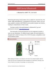
Clike here to get datasheet of CC1101 - Elechouse
Clike here to get datasheet of CC1101 - Elechouse
Clike here to get datasheet of CC1101 - Elechouse

You also want an ePaper? Increase the reach of your titles
YUMPU automatically turns print PDFs into web optimized ePapers that Google loves.
6789<strong>CC1101</strong><strong>CC1101</strong>Low-Cost Low-Power Sub-1GHz RF Transceiver(Enhanced CC1100 )Applications• Ultra low-power wireless applicationsoperating in the 315/433/868/915 MHzISM/SRD bands• Wireless alarm and security systems• Industrial moni<strong>to</strong>ring and controlProduct DescriptionThe <strong>CC1101</strong> is a low-cost sub- 1 GHztransceiver designed for very low-powerwireless applications. The circuit is mainlyintended for the ISM (Industrial, Scientific andMedical) and SRD (Short Range Device)frequency bands at 315, 433, 868, and 915MHz, but can easily be programmed foroperation at other frequencies in the 300-348MHz, 387-464 MHz and 779-928 MHz bands.<strong>CC1101</strong> is an improved and code compatibleversion <strong>of</strong> the CC1100 RF transceiver. Themain improvements on the <strong>CC1101</strong> include:• Improved spurious response• Better close-in phase noise improvingAdjacent Channel Power (ACP)performance• Higher input saturation level• Improved output power ramping• Extended frequency bands <strong>of</strong>operation, i.e.CC1100: 400-464 MHz and 800-928MHz<strong>CC1101</strong>: 387-464 MHz and 779-928MHz• Wireless sensor networks• AMR – Au<strong>to</strong>matic Meter Reading• Home and building au<strong>to</strong>mationThe RF transceiver is integrated with a highlyconfigurable baseband modem. The modemsupports various modulation formats and hasa configurable data rate up <strong>to</strong> 500 kBaud.<strong>CC1101</strong> provides extensive hardware supportfor packet handling, data buffering, bursttransmissions, clear channel assessment, linkquality indication, and wake-on-radio.The main operating parameters and the 64-byte transmit/receive FIFOs <strong>of</strong> <strong>CC1101</strong> can becontrolled via an SPI interface. In a typicalsystem, the <strong>CC1101</strong> will be used <strong>to</strong><strong>get</strong>her with amicrocontroller and a few additional passivecomponents.1234520191817<strong>CC1101</strong>16101514131211This product shall not be used in any <strong>of</strong> the following products or systems without prior express written permission fromTexas Instruments:(i)(ii)(iii)implantable cardiac rhythm management systems, including without limitation pacemakers,defibrilla<strong>to</strong>rs and cardiac resynchronization devices,external cardiac rhythm management systems that communicate directly with one or more implantablemedical devices; orother devices used <strong>to</strong> moni<strong>to</strong>r or treat cardiac function, including without limitation pressure sensors,biochemical sensors and neurostimula<strong>to</strong>rs.Please contact lpw-medical-approval@list.ti.com if your application might fall within the category described above.SWRS061C Page 1 <strong>of</strong> 94
<strong>CC1101</strong>Key FeaturesRF Performance• High sensitivity (–111 dBm at 1.2 kBaud,868 MHz, 1% packet error rate)• Low current consumption (14.7 mA in RX,1.2 kBaud, 868 MHz)• Programmable output power up <strong>to</strong> +10dBm for all supported frequencies• Excellent receiver selectivity and blockingperformance• Programmable data rate from 1.2 <strong>to</strong> 500kBaud• Frequency bands: 300-348 MHz, 387-464MHz and 779-928 MHzAnalog Features• 2-FSK, GFSK, and MSK supported as wellas OOK and flexible ASK shaping• Suitable for frequency hopping systemsdue <strong>to</strong> a fast settling frequencysynthesizer: 90us settling time• Au<strong>to</strong>matic Frequency Compensation(AFC) can be used <strong>to</strong> align the frequencysynthesizer <strong>to</strong> the received centerfrequency• Integrated analog temperature sensorDigital Features• Flexible support for packet orientedsystems: On-chip support for sync worddetection, address check, flexible packetlength, and au<strong>to</strong>matic CRC handling• Efficient SPI interface: All registers can beprogrammed with one “burst” transfer• Digital RSSI output• Programmable channel filter bandwidth• Programmable Carrier Sense (CS)indica<strong>to</strong>r• Programmable Preamble Quality Indica<strong>to</strong>r(PQI) for improved protection against falsesync word detection in random noise• Support for au<strong>to</strong>matic Clear ChannelAssessment (CCA) before transmitting (forlisten-before-talk systems)• Support for per-package Link QualityIndication (LQI)• Optional au<strong>to</strong>matic whitening and dewhitening<strong>of</strong> dataLow-Power Features• 400 nA sleep mode current consumption• Fast startup time: 240us from sleep <strong>to</strong> RXor TX mode (measured on EM referencedesign [5] and [6])• Wake-on-radio functionality for au<strong>to</strong>maticlow-power RX polling• Separate 64-byte RX and TX data FIFOs(enables burst mode data transmission)General• Few external components: Completely onchipfrequency synthesizer, no externalfilters or RF switch needed• Green package: RoHS compliant and noantimony or bromine• Small size (QLP 4x4 mm package, 20pins)• Suited for systems tar<strong>get</strong>ing compliancewith EN 300 220 (Europe) and FCC CFRPart 15 (US).• Support for asynchronous andsynchronous serial receive/transmit modefor backwards compatibility with existingradio communication pro<strong>to</strong>colsSWRS061C Page 2 <strong>of</strong> 94
<strong>CC1101</strong>AbbreviationsAbbreviations used in this data sheet are described below.ACP Adjacent Channel Power MSK Minimum Shift KeyingADC Analog <strong>to</strong> Digital Converter N/A Not ApplicableAFC Au<strong>to</strong>matic Frequency Compensation NRZ Non Return <strong>to</strong> Zero (Coding)AGC Au<strong>to</strong>matic Gain Control OOK On-Off KeyingAMR Au<strong>to</strong>matic Meter Reading PA Power AmplifierASK Amplitude Shift Keying PCB Printed Circuit BoardBER Bit Error Rate PD Power DownBT Bandwidth-Time product PER Packet Error RateCCA Clear Channel Assessment PLL Phase Locked LoopCFR Code <strong>of</strong> Federal Regulations POR Power-On ResetCRC Cyclic Redundancy Check PQI Preamble Quality Indica<strong>to</strong>rCS Carrier Sense PQT Preamble Quality ThresholdCW Continuous Wave (Unmodulated Carrier) PTAT Proportional To Absolute TemperatureDC Direct Current QLP Quad Leadless PackageDVGA Digital Variable Gain Amplifier QPSK Quadrature Phase Shift KeyingESR Equivalent Series Resistance RC Resis<strong>to</strong>r-Capaci<strong>to</strong>rFCC Federal Communications Commission RF Radio FrequencyFEC Forward Error Correction RSSI Received Signal Strength Indica<strong>to</strong>rFIFO First-In-First-Out RX Receive, Receive ModeFHSS Frequency Hopping Spread Spectrum SAW Surface Aqustic Wave2-FSK Binary Frequency Shift Keying SMD Surface Mount DeviceGFSK Gaussian shaped Frequency Shift Keying SNR Signal <strong>to</strong> Noise RatioIF Intermediate Frequency SPI Serial Peripheral InterfaceI/Q In-Phase/Quadrature SRD Short Range DevicesISM Industrial, Scientific, Medical TBD To Be DefinedLC Induc<strong>to</strong>r-Capaci<strong>to</strong>r T/R Transmit/ReceiveLNA Low Noise Amplifier TX Transmit, Transmit ModeLO Local Oscilla<strong>to</strong>r UHF Ultra High frequencyLSB Least Significant Bit VCO Voltage Controlled Oscilla<strong>to</strong>rLQI Link Quality Indica<strong>to</strong>r WOR Wake on Radio, Low power pollingMCU Microcontroller Unit XOSC Crystal Oscilla<strong>to</strong>rMSB Most Significant Bit XTAL CrystalSWRS061C Page 3 <strong>of</strong> 94
<strong>CC1101</strong>Table Of ContentsAPPLICATIONS..................................................................................................................................................1PRODUCT DESCRIPTION................................................................................................................................1KEY FEATURES .................................................................................................................................................1KEY FEATURES .................................................................................................................................................2RF PERFORMANCE ..........................................................................................................................................2ANALOG FEATURES ........................................................................................................................................2DIGITAL FEATURES.........................................................................................................................................2LOW-POWER FEATURES................................................................................................................................2GENERAL ............................................................................................................................................................2ABBREVIATIONS...............................................................................................................................................3TABLE OF CONTENTS .....................................................................................................................................41 ABSOLUTE MAXIMUM RATINGS.....................................................................................................72 OPERATING CONDITIONS .................................................................................................................73 GENERAL CHARACTERISTICS.........................................................................................................74 ELECTRICAL SPECIFICATIONS .......................................................................................................84.1 CURRENT CONSUMPTION ............................................................................................................................84.2 RF RECEIVE SECTION................................................................................................................................104.3 RF TRANSMIT SECTION .............................................................................................................................124.4 CRYSTAL OSCILLATOR..............................................................................................................................134.5 LOW POWER RC OSCILLATOR...................................................................................................................144.6 FREQUENCY SYNTHESIZER CHARACTERISTICS..........................................................................................144.7 ANALOG TEMPERATURE SENSOR ..............................................................................................................154.8 DC CHARACTERISTICS ..............................................................................................................................154.9 POWER-ON RESET.....................................................................................................................................155 PIN CONFIGURATION........................................................................................................................166 CIRCUIT DESCRIPTION ....................................................................................................................177 APPLICATION CIRCUIT ....................................................................................................................188 CONFIGURATION OVERVIEW........................................................................................................219 CONFIGURATION SOFTWARE........................................................................................................2310 4-WIRE SERIAL CONFIGURATION AND DATA INTERFACE ..................................................2310.1 CHIP STATUS BYTE ...................................................................................................................................2510.2 REGISTER ACCESS.....................................................................................................................................2510.3 SPI READ ..................................................................................................................................................2610.4 COMMAND STROBES .................................................................................................................................2610.5 FIFO ACCESS ............................................................................................................................................2610.6 PATABLE ACCESS...................................................................................................................................2711 MICROCONTROLLER INTERFACE AND PIN CONFIGURATION ..........................................2711.1 CONFIGURATION INTERFACE.....................................................................................................................2711.2 GENERAL CONTROL AND STATUS PINS .....................................................................................................2711.3 OPTIONAL RADIO CONTROL FEATURE ......................................................................................................2812 DATA RATE PROGRAMMING..........................................................................................................2813 RECEIVER CHANNEL FILTER BANDWIDTH ..............................................................................3014 DEMODULATOR, SYMBOL SYNCHRONIZER, AND DATA DECISION..................................3014.1 FREQUENCY OFFSET COMPENSATION........................................................................................................3014.2 BIT SYNCHRONIZATION.............................................................................................................................3014.3 BYTE SYNCHRONIZATION..........................................................................................................................3115 PACKET HANDLING HARDWARE SUPPORT ..............................................................................3115.1 DATA WHITENING.....................................................................................................................................3215.2 PACKET FORMAT.......................................................................................................................................32SWRS061C Page 4 <strong>of</strong> 94
<strong>CC1101</strong>15.3 PACKET FILTERING IN RECEIVE MODE......................................................................................................3415.4 PACKET HANDLING IN TRANSMIT MODE...................................................................................................3415.5 PACKET HANDLING IN RECEIVE MODE .....................................................................................................3515.6 PACKET HANDLING IN FIRMWARE.............................................................................................................3516 MODULATION FORMATS.................................................................................................................3616.1 FREQUENCY SHIFT KEYING.......................................................................................................................3616.2 MINIMUM SHIFT KEYING...........................................................................................................................3616.3 AMPLITUDE MODULATION ........................................................................................................................3617 RECEIVED SIGNAL QUALIFIERS AND LINK QUALITY INFORMATION ............................3717.1 SYNC WORD QUALIFIER............................................................................................................................3717.2 PREAMBLE QUALITY THRESHOLD (PQT) ..................................................................................................3717.3 RSSI..........................................................................................................................................................3717.4 CARRIER SENSE (CS).................................................................................................................................3917.5 CLEAR CHANNEL ASSESSMENT (CCA) .....................................................................................................4017.6 LINK QUALITY INDICATOR (LQI)..............................................................................................................4018 FORWARD ERROR CORRECTION WITH INTERLEAVING .....................................................4018.1 FORWARD ERROR CORRECTION (FEC)......................................................................................................4018.2 INTERLEAVING ..........................................................................................................................................4119 RADIO CONTROL................................................................................................................................4219.1 POWER-ON START-UP SEQUENCE.............................................................................................................4219.2 CRYSTAL CONTROL...................................................................................................................................4319.3 VOLTAGE REGULATOR CONTROL..............................................................................................................4419.4 ACTIVE MODES .........................................................................................................................................4419.5 WAKE ON RADIO (WOR)..........................................................................................................................4419.6 TIMING ......................................................................................................................................................4519.7 RX TERMINATION TIMER ..........................................................................................................................4620 DATA FIFO ............................................................................................................................................4621 FREQUENCY PROGRAMMING........................................................................................................482222.1VCO .........................................................................................................................................................48VCO AND PLL SELF-CALIBRATION ..........................................................................................................4823 VOLTAGE REGULATORS .................................................................................................................4924 OUTPUT POWER PROGRAMMING ................................................................................................4925 SHAPING AND PA RAMPING............................................................................................................5026 SELECTIVITY.......................................................................................................................................522727.1CRYSTAL OSCILLATOR....................................................................................................................53REFERENCE SIGNAL ..................................................................................................................................5428 EXTERNAL RF MATCH .....................................................................................................................5429 PCB LAYOUT RECOMMENDATIONS.............................................................................................5430 GENERAL PURPOSE / TEST OUTPUT CONTROL PINS .............................................................5531 ASYNCHRONOUS AND SYNCHRONOUS SERIAL OPERATION ..............................................5731.1 ASYNCHRONOUS OPERATION ....................................................................................................................5731.2 SYNCHRONOUS SERIAL OPERATION ..........................................................................................................5732 SYSTEM CONSIDERATIONS AND GUIDELINES .........................................................................5732.1 SRD REGULATIONS...................................................................................................................................5732.2 FREQUENCY HOPPING AND MULTI-CHANNEL SYSTEMS............................................................................5832.3 WIDEBAND MODULATION NOT USING SPREAD SPECTRUM........................................................................5832.4 DATA BURST TRANSMISSIONS...................................................................................................................5832.5 CONTINUOUS TRANSMISSIONS ..................................................................................................................5932.6 CRYSTAL DRIFT COMPENSATION ..............................................................................................................5932.7 SPECTRUM EFFICIENT MODULATION.........................................................................................................5932.8 LOW COST SYSTEMS .................................................................................................................................5932.9 BATTERY OPERATED SYSTEMS .................................................................................................................5932.10 INCREASING OUTPUT POWER ................................................................................................................59SWRS061C Page 5 <strong>of</strong> 94
<strong>CC1101</strong>33 CONFIGURATION REGISTERS........................................................................................................6033.1 CONFIGURATION REGISTER DETAILS – REGISTERS WITH PRESERVED VALUES IN SLEEP STATE...............6433.2 CONFIGURATION REGISTER DETAILS – REGISTERS THAT LOOSE PROGRAMMING IN SLEEP STATE .........8433.3 STATUS REGISTER DETAILS.......................................................................................................................8534 PACKAGE DESCRIPTION (QLP 20).................................................................................................8834.1 RECOMMENDED PCB LAYOUT FOR PACKAGE (QLP 20) ...........................................................................8934.2 PACKAGE THERMAL PROPERTIES ..............................................................................................................8934.3 SOLDERING INFORMATION ........................................................................................................................8934.4 TRAY SPECIFICATION ................................................................................................................................8934.5 CARRIER TAPE AND REEL SPECIFICATION.................................................................................................9035 ORDERING INFORMATION..............................................................................................................9036 REFERENCES .......................................................................................................................................9137 GENERAL INFORMATION................................................................................................................9237.1 DOCUMENT HISTORY ................................................................................................................................9237.2 PRODUCT STATUS DEFINITIONS ................................................................................................................9238 ADDRESS INFORMATION.................................................................................................................9339 TI WORLDWIDE TECHNICAL SUPPORT......................................................................................93SWRS061C Page 6 <strong>of</strong> 94
<strong>CC1101</strong>1 Absolute Maximum RatingsUnder no circumstances must the absolute maximum ratings given in Table 1 be violated. Stressexceeding one or more <strong>of</strong> the limiting values may cause permanent damage <strong>to</strong> the device.Caution! ESD sensitive device.Precaution should be used when handlingthe device in order <strong>to</strong> prevent permanentdamage.Parameter Min Max Units ConditionSupply voltage –0.3 3.9 V All supply pins must have the same voltageVoltage on any digital pin –0.3 VDD + 0.3max 3.9Voltage on the pins RF_P, RF_N,and DCOUPL–0.3 2.0 VVoltage ramp-up rate 120 kV/µsInput RF level +10 dBmS<strong>to</strong>rage temperature range –50 150 °CSolder reflow temperature 260 °C According <strong>to</strong> IPC/JEDEC J-STD-020CESD 750 V According <strong>to</strong> JEDEC STD 22, method A114,Human Body Model (HBM)ESD 400 V According <strong>to</strong> JEDEC STD 22, C101C,Charged Device Model (CDM)Table 1: Absolute Maximum RatingsV2 Operating ConditionsThe operating conditions for <strong>CC1101</strong> are listed Table 2 in below.Parameter Min Max Unit ConditionOperating temperature -40 85 °COperating supply voltage 1.8 3.6 V All supply pins must have the same voltageTable 2: Operating Conditions3 General CharacteristicsParameter Min Typ Max Unit Condition/NoteFrequency range 300 348 MHz387 464 MHz779 928 MHzData rate 1.2500kBaud2-FSK1.2250kBaudGFSK, OOK, and ASK26500kBaud(Shaped) MSK (also known as differential <strong>of</strong>fsetQPSK)Optional Manchester encoding (the data rate in kbpswill be half the baud rate)Table 3: General CharacteristicsSWRS061C Page 7 <strong>of</strong> 94
<strong>CC1101</strong>4 Electrical Specifications4.1 Current ConsumptionTc = 25°C, VDD = 3.0V if nothing else stated. All measurement results are obtained using the <strong>CC1101</strong>EM reference designs([5] and [6]).Reduced current settings (MDMCFG2.DEM_DCFILT_OFF=1) gives a slightly lower current consumption at the cost <strong>of</strong> areduction in sensitivity. Seefor additional details on current consumption and sensitivity.Parameter Min Typ Max Unit ConditionCurrent consumption in powerdown modes0.2 1 µA Voltage regula<strong>to</strong>r <strong>to</strong> digital part <strong>of</strong>f, register values retained(SLEEP state). All GDO pins programmed <strong>to</strong> 0x2F (HW <strong>to</strong> 0)0.5 µA Voltage regula<strong>to</strong>r <strong>to</strong> digital part <strong>of</strong>f, register values retained, lowpowerRC oscilla<strong>to</strong>r running (SLEEP state with WOR enabled100 µA Voltage regula<strong>to</strong>r <strong>to</strong> digital part <strong>of</strong>f, register values retained,XOSC running (SLEEP state with MCSM0.OSC_FORCE_ON set)165 µA Voltage regula<strong>to</strong>r <strong>to</strong> digital part on, all other modules in powerdown (XOFF state)Current consumption9.8 µA Au<strong>to</strong>matic RX polling once each second, using low-power RCoscilla<strong>to</strong>r, with 460 kHz filter bandwidth and 250 kBaud data rate,PLL calibration every 4 th wakeup. Average current with signal inchannel below carrier sense level (MCSM2.RX_TIME_RSSI=1).34.2 µA Same as above, but with signal in channel above carrier senselevel, 1.95 ms RX timeout, and no preamble/sync word found.1.5 µA Au<strong>to</strong>matic RX polling every 15 th second, using low-power RCoscilla<strong>to</strong>r, with 460kHz filter bandwidth and 250 kBaud data rate,PLL calibration every 4 th wakeup. Average current with signal inchannel below carrier sense level (MCSM2.RX_TIME_RSSI=1).39.3 µA Same as above, but with signal in channel above carrier senselevel, 29.3 ms RX timeout, and no preamble/sync word found.1.7 mA Only voltage regula<strong>to</strong>r <strong>to</strong> digital part and crystal oscilla<strong>to</strong>r running(IDLE state)8.4 mA Only the frequency synthesizer is running (FSTXON state). Thiscurrents consumption is also representative for the otherintermediate states when going from IDLE <strong>to</strong> RX or TX, includingthe calibration state.Current consumption,315MHz15.4 mA Receive mode, 1.2 kBaud, reduced current, input at sensitivitylimit14.4 mA Receive mode, 1.2 kBaud, reduced current, input well abovesensitivity limit15.2 mA Receive mode, 38.4 kBaud, reduced current, input at sensitivitylimit14.3 mA Receive mode,38.4 kBaud, reduced current, input well abovesensitivity limit16.5 mA Receive mode, 250 kBaud, reduced current, input at sensitivitylimit15.1 mA Receive mode, 250 kBaud, reduced current, input well abovesensitivity limit27.4 mA Transmit mode, +10 dBm output power15.0 mA Transmit mode, 0 dBm output power12.3 mA Transmit mode, –6 dBm output powerSWRS061C Page 8 <strong>of</strong> 94
<strong>CC1101</strong>Parameter Min Typ Max Unit ConditionCurrent consumption,433MHzCurrent consumption,868/915MHz16.0 mA Receive mode, 1.2 kBaud, reduced current, input at sensitivitylimit15.0 mA Receive mode, 1.2 kBaud, reduced current, input well abovesensitivity limit15.7 mA Receive mode, 38.4 kBaud , reduced current, input at sensitivitylimit15.0 mA Receive mode, 38.4 kBaud , reduced current, input well abovesensitivity limit17.1 mA Receive mode, 250 kBaud, reduced current, input at sensitivitylimit15.7 mA Receive mode, 250 kBaud, reduced current, input well abovesensitivity limit29.2 mA Transmit mode, +10 dBm output power16.0 mA Transmit mode, 0 dBm output power13.1 mA Transmit mode, –6 dBm output power15.7 mA Receive mode, 1.2 kBaud , reduced current, input at sensitivitylimit14.7 mA Receive mode, 1.2 kBaud , reduced current, input well abovesensitivity limit15.6 mA Receive mode, 38.4 kBaud , reduced current, input at sensitivitylimit14.6 mA Receive mode, 38.4 kBaud , reduced current, input well abovesensitivity limit16.9 mA Receive mode, 250 kBaud , reduced current, input at sensitivitylimit15.6 mA Receive mode, 250 kBaud , reduced current, input well abovesensitivity limit32.3 mA Transmit mode, +10 dBm output power16.8 mA Transmit mode, 0 dBm output power13.1 mA Transmit mode, –6 dBm output powerTable 4: Electrical SpecificationsSWRS061C Page 9 <strong>of</strong> 94
<strong>CC1101</strong>4.2 RF Receive SectionTc = 25°C, VDD = 3.0V if nothing else stated. All measurement results are obtained using the <strong>CC1101</strong>EM reference designs( [5] and [6]).Parameter Min Typ Max Unit Condition/NoteDigital channel filterbandwidth58 812 kHz User programmable. The bandwidth limits are proportional <strong>to</strong>crystal frequency (given values assume a 26.0 MHz crystal).315 MHz, 1.2 kBaud data rate, sensitivity optimized, MDMCFG2.DEM_DCFILT_OFF=0(2-FSK, 1% packet error rate, 20 bytes packet length, 5.2 kHz deviation, 58 kHz digital channel filter bandwidth)Receiver sensitivity -111 dBm Sensitivity can be traded for current consumption by settingMDMCFG2.DEM_DCFILT_OFF=1. The typical currentconsumption is then reduced from 17.2 mA <strong>to</strong> 15.4 mA atsensitivity limit. The sensitivity is typically reduced <strong>to</strong> -109 dBm315 MHz, 500 kBaud data rate, sensitivity optimized, MDMCFG2.DEM_DCFILT_OFF=0 (MDMCFG2.DEM_DCFILT_OFF=1cannot be used for data rates > 250 kBaud)(MSK, 1% packet error rate, 20 bytes packet length, 812 kHz digital channel filter bandwidth)-88 dBm433 MHz, 1.2 kBaud data rate, sensitivity optimized, MDMCFG2.DEM_DCFILT_OFF=0(GFSK, 1% packet error rate, 20 bytes packet length, 5.2 kHz deviation, 58 kHz digital channel filter bandwidthReceiver sensitivity -112 dBm Sensitivity can be traded for current consumption by settingMDMCFG2.DEM_DCFILT_OFF=1. The typical currentconsumption is then reduced from 18.0 mA <strong>to</strong> 16.0 mA atsensitivity limit. The sensitivity is typically reduced <strong>to</strong> -110 dBm433 MHz, 38.4 kBaud data rate, sensitivity optimized, MDMCFG2.DEM_DCFILT_OFF=0(GFSK, 1% packet error rate, 20 bytes packet length, 20 kHz deviation, 100 kHz digital channel filter bandwidth)Receiver sensitivity –104 dBm433 MHz, 250 kBaud data rate, sensitivity optimized, MDMCFG2.DEM_DCFILT_OFF=0(MSK, 1% packet error rate, 20 bytes packet length, 127 kHz deviation, 540 kHz digital channel filter bandwidth)Receiver sensitivity -95 dBm868 MHz, 1.2 kBaud data rate, sensitivity optimized, MDMCFG2.DEM_DCFILT_OFF=0(2-FSK, 1% packet error rate, 20 bytes packet length, 5.2 kHz deviation, 58 kHz digital channel filter bandwidth)Receiver sensitivity –111 dBm Sensitivity can be traded for current consumption by settingMDMCFG2.DEM_DCFILT_OFF=1. The typical currentconsumption is then reduced from 18.0 mA <strong>to</strong> 15.7 mA atsensitivity limit. The sensitivity is typically reduced <strong>to</strong> -109 dBmSaturation –14 dBm FIFOTHR.CLOSE_IN_RX=0Adjacent channelrejectionAlternate channelrejectionImage channelrejection,868MHz37 dB Desired channel 3 dB above the sensitivity limit. 100 kHzchannel spacing37 dB Desired channel 3 dB above the sensitivity limit. 100 kHzchannel spacingSee Figure 24 for plot <strong>of</strong> selectivity versus frequency <strong>of</strong>fset31 dB IF frequency 152 kHzDesired channel 3 dB above the sensitivity limit.868 MHz, 38.4 kBaud data rate, sensitivity optimized(GFSK, 1% packet error rate, 20 bytes packet length, 20 kHz deviation, 100 kHz digital channel filter bandwidth)Receiver sensitivity –103 dBmSaturation –16 dBmAdjacent channelrejectionAlternate channelrejectionImage channelrejection,868MHz20 dB Desired channel 3 dB above the sensitivity limit. 200 kHzchannel spacing30 dB Desired channel 3 dB above the sensitivity limit. 200 kHzchannel spacingSee Figure 25 for plot <strong>of</strong> selectivity versus frequency <strong>of</strong>fset23 dB IF frequency 152 kHzDesired channel 3 dB above the sensitivity limit.SWRS061C Page 10 <strong>of</strong> 94
<strong>CC1101</strong>Parameter Min Typ Max Unit Condition/Note868 MHz, 250 kBaud data rate, sensitivity optimized, MDMCFG2.DEM_DCFILT_OFF=0(MSK, 1% packet error rate, 20 bytes packet length, 540 kHz digital channel filter bandwidth)Receiver sensitivity –94 dBm Sensitivity can be traded for current consumption by settingMDMCFG2.DEM_DCFILT_OFF=1. The typical currentconsumption is then reduced from 19.2 mA <strong>to</strong> 16.9 mA atsensitivity limit. The sensitivity is typically reduced <strong>to</strong> -91 dBmSaturation –17 dBm FIFOTHR.CLOSE_IN_RX=0Adjacent channel rejection 25 dB Desired channel 3 dB above the sensitivity limit. 750 kHzchannel spacingAlternate channelrejectionImage channel rejection,868MHz40 dB Desired channel 3 dB above the sensitivity limit. 750 kHzchannel spacingSee Figure 26 for plot <strong>of</strong> selectivity versus frequency <strong>of</strong>fset17 dB IF frequency 304 kHzDesired channel 3 dB above the sensitivity limit.915 MHz, 1.2 kBaud data rate, sensitivity optimized, MDMCFG2.DEM_DCFILT_OFF=0(2-FSK, 5.2kHz deviation, 1% packet error rate, 20 bytes packet length, 58 kHz digital channel filter bandwidth)Receiver sensitivity –111 dBm Sensitivity can be traded for current consumption by settingMDMCFG2.DEM_DCFILT_OFF=1. The typical currentconsumption is then reduced from 18.0 mA <strong>to</strong> 15.7 mA atsensitivity limit. The sensitivity is typically reduced <strong>to</strong> -109dBm915 MHz, 38.4 kBaud data rate, sensitivity optimized, MDMCFG2.DEM_DCFILT_OFF=0(2-FSK, 1% packet error rate, 20 bytes packet length, 20 kHz deviation, 100 kHz digital channel filter bandwidth)Receiver sensitivity –103 dBm915 MHz, 250 kBaud data rate, sensitivity optimized, MDMCFG2.DEM_DCFILT_OFF=0(MSK, 1% packet error rate, 20 bytes packet length, 540 kHz digital channel filter bandwidth)Receiver sensitivity –94 dBm Sensitivity can be traded for current consumption by settingMDMCFG2.DEM_DCFILT_OFF=1. The typical currentconsumption is then reduced from 19.2 mA <strong>to</strong> 16.9 mA atsensitivity limit. The sensitivity is typically reduced <strong>to</strong> -91 dBm915 MHz, 500 kBaud data rate, sensitivity optimized, MDMCFG2.DEM_DCFILT_OFF=0 (MDMCFG2.DEM_DCFILT_OFF=1cannot be used for data rates > 250 kBaud)(MSK, 1% packet error rate, 20 bytes packet length, 812 kHz digital channel filter bandwidth)Receiver sensitivity –87 dBmBlockingBlocking at ±2 MHz <strong>of</strong>fset,1.2 kBaud, 868 MHzBlocking at ±2 MHz <strong>of</strong>fset,500 kBaud, 868 MHzBlocking at ±10 MHz<strong>of</strong>fset, 1.2 kBaud, 868MHzBlocking at ±10 MHz<strong>of</strong>fset, 500 kBaud, 868MHz-50 dBm Desired channel 3dB above the sensitivity limit.-50 dBm Desired channel 3dB above the sensitivity limit-39 dBm Desired channel 3dB above the sensitivity limit.-40 dBm Desired channel 3dB above the sensitivity limit.SWRS061C Page 11 <strong>of</strong> 94
<strong>CC1101</strong>Parameter Min Typ Max Unit Condition/NoteGeneralSpurious emissions -68-66–57–47dBmdBmTable 5: RF Receive Section25 MHz – 1 GHz(Maximum figure is the ETSI EN 300 220 limit)Above 1 GHz(Maximum figure is the ETSI EN 300 220 limit)Typical radiated spurious emission is -49 dBmeasured at the VCO frequency.RX latency 9 bit Serial operation. Time from start <strong>of</strong> reception untildata is available on the receiver data output pin isequal <strong>to</strong> 9 bit.4.3 RF Transmit SectionTc = 25°C, VDD = 3.0V, +10dBm if nothing else stated. All measurement results are obtained using the <strong>CC1101</strong>EM referencedesigns ( [5] and [6]).Parameter Min Typ Max Unit Condition/NoteDifferential loadimpedance315 MHz433 MHz868/915 MHzOutput power,highest settingOutput power,lowest setting122 + j31116 + j4186.5 + j43ΩDifferential impedance as seen from the RF-port (RF_P andRF_N) <strong>to</strong>wards the antenna. Follow the <strong>CC1101</strong>EM referencedesign ( [5] and [6]) available from theTI website.+10 dBm Output power is programmable, and full range is available in allfrequency bands(Output power may be restricted by regula<strong>to</strong>ry limits. See alsoApplication Note AN039 [3].Delivered <strong>to</strong> a 50Ω single-ended load via <strong>CC1101</strong>EM referencedesign ( [5] and [6]) RF matching network.-30 dBm Output power is programmable, and full range is available in allfrequency bands.Delivered <strong>to</strong> a 50Ω single-ended load via <strong>CC1101</strong>EM referencedesign( [5] and [6]) RF matching network.Harmonics,radiatedMeasured on <strong>CC1101</strong>EM reference designs( [5] and [6]) with CW,10dBm output power2 nd Harm, 433 MHz3 rd Harm, 433 MHz-49-40dBmThe antennas used during the radiated measurements (SMAFF-433 from R.W.Badland and Nearson S331 868/915) play a part inattenuating the harmonics2 nd Harm, 868 MHz3 rd Harm, 868 MHz-39-64Harmonics,conductedMeasured with 10 dBm CW, TX frequency at 315.00 MHz,433.00 MHz, 868.00 MHz, or 915.00 MHz315 MHz< -35< -53dBmFrequencies below 960 MHzFrequencies above 960 MHz433 MHz< -43< -45Frequencies below 1 GHzFrequencies above 1 GHz868 MHz< -39915 MHz< -33SWRS061C Page 12 <strong>of</strong> 94
<strong>CC1101</strong>Parameter Min Typ Max Unit Condition/NoteSpuriousemissions,conductedHarmonics notincluded315 MHz< -58< -53dBmMeasured with 10 dBm CW, TX frequency at 315.00 MHz,433.00 MHz, 868.00 MHz or 915.00 MHzFrequencies below 960 MHzFrequencies above 960 MHz433 MHz< -50< -54< -56Frequencies below 1 GHzFrequencies above 1 GHzFrequencies within 47-74, 87.5-118, 174-230, 470-862 MHz868 MHz915 MHzGeneral< -50< -51< -53< -51< -51Frequencies below 1 GHzFrequencies above 1 GHzFrequencies within 47-74, 87.5-118, 174-230, 470-862 MHz.All radiated spurious emissions are within the limits <strong>of</strong> ETSI. Thepeak conducted spurious emission is -53 dBm at 699 MHz, whichis in a frequency band limited <strong>to</strong> -54 dBm by EN 300 220. Analternative filter that can be used <strong>to</strong> reduce the emission at 699MHz below -54 dBm, for conducted measurements, is shown inFigure 4.Frequencies below 960 MHzFrequencies above 960 MHzTX latency 8 bit Serial operation. Time from sampling the data on the transmitterdata input pin until it is observed on the RF output ports.Table 6: RF Transmit Section4.4 Crystal Oscilla<strong>to</strong>rTc = 25°C @ VDD = 3.0 V if nothing else is stated.Parameter Min Typ Max Unit Condition/NoteCrystal frequency 26 26 27 MHzTolerance ±40 ppm This is the <strong>to</strong>tal <strong>to</strong>lerance including a) initial <strong>to</strong>lerance, b) crystalloading, c) aging, and d) temperature dependence.The acceptable crystal <strong>to</strong>lerance depends on RF frequency andchannel spacing / bandwidth.ESR 100 ΩStart-up time 150 µs Measured on the <strong>CC1101</strong>EM reference designs ([5] and [6])using crystal AT-41CD2 from NDK.This parameter is <strong>to</strong> a large degree crystal dependent.Table 7: Crystal Oscilla<strong>to</strong>r ParametersSWRS061C Page 13 <strong>of</strong> 94
<strong>CC1101</strong>4.5 Low Power RC Oscilla<strong>to</strong>rTc = 25°C, VDD = 3.0 V if nothing else is stated. All measurement results obtained using the <strong>CC1101</strong>EM reference designs ( [5]and [6]).Parameter Min Typ Max Unit Condition/NoteCalibrated frequency 34.7 34.7 36 kHz Calibrated RC Oscilla<strong>to</strong>r frequency is XTALfrequency divided by 750Frequency accuracy aftercalibration±1 %Temperature coefficient +0.5 % / °C Frequency drift when temperature changes aftercalibrationSupply voltage coefficient +3 % / V Frequency drift when supply voltage changes aftercalibrationInitial calibration time 2 ms When the RC Oscilla<strong>to</strong>r is enabled, calibration iscontinuously done in the background as long asthe crystal oscilla<strong>to</strong>r is running.Table 8: RC Oscilla<strong>to</strong>r Parameters4.6 Frequency Synthesizer CharacteristicsTc = 25°C @ VDD = 3.0 V if nothing else is stated. All measurement results are obtained using the <strong>CC1101</strong>EM referencedesigns ( [5] and [6]). Min figures are given using a 27 MHz crystal. Typ and max are given using a 26 MHz crystal.Parameter Min Typ Max Unit Condition/NoteProgrammed frequencyresolutionSynthesizer frequency<strong>to</strong>lerance412 Hz 26-27 MHz crystal.397 F XOSC /2 16 The resolution (in Hz) is equal for all frequencybands.±40 ppm Given by crystal used. Required accuracy(including temperature and aging) depends onfrequency band and channel bandwidth /spacing.RF carrier phase noise –92 dBc/Hz @ 50 kHz <strong>of</strong>fset from carrierRF carrier phase noise –92 dBc/Hz @ 100 kHz <strong>of</strong>fset from carrierRF carrier phase noise –92 dBc/Hz @ 200 kHz <strong>of</strong>fset from carrierRF carrier phase noise –98 dBc/Hz @ 500 kHz <strong>of</strong>fset from carrierRF carrier phase noise –107 dBc/Hz @ 1 MHz <strong>of</strong>fset from carrierRF carrier phase noise –113 dBc/Hz @ 2 MHz <strong>of</strong>fset from carrierRF carrier phase noise –119 dBc/Hz @ 5 MHz <strong>of</strong>fset from carrierRF carrier phase noise –129 dBc/Hz @ 10 MHz <strong>of</strong>fset from carrierPLL turn-on / hop time 85.1 88.4 88.4 µs Time from leaving the IDLE state until arriving inthe RX, FSTXON or TX state, when notperforming calibration.Crystal oscilla<strong>to</strong>r running.PLL RX/TX settling time 9.3 9.6 9.6 µs Settling time for the 1·IF frequency step from RX<strong>to</strong> TXPLL TX/RX settling time 20.7 21.5 21.5 µs Settling time for the 1·IF frequency step from TX<strong>to</strong> RXPLL calibration time 694 721 721 µs Calibration can be initiated manually orau<strong>to</strong>matically before entering or after leavingRX/TX.Table 9: Frequency Synthesizer ParametersSWRS061C Page 14 <strong>of</strong> 94
<strong>CC1101</strong>4.7 Analog Temperature SensorThe characteristics <strong>of</strong> the analog temperature sensor at 3.0 V supply voltage are listed in Table 10below. Note that it is necessary <strong>to</strong> write 0xBF <strong>to</strong> the PTEST register <strong>to</strong> use the analog temperaturesensor in the IDLE state.Parameter Min Typ Max Unit Condition/NoteOutput voltage at –40°C 0.651 VOutput voltage at 0°C 0.747 VOutput voltage at +40°C 0.847 VOutput voltage at +80°C 0.945 VTemperature coefficient 2.45 mV/°C Fitted from –20 °C <strong>to</strong> +80 °CError in calculatedtemperature, calibratedCurrent consumptionincrease when enabled-2 * 0 2 * °C From –20 °C <strong>to</strong> +80 °C when using 2.45 mV / °C, after1-point calibration at room temperature0.3 mA* The indicated minimum and maximum error with 1-point calibration is based on simulated values fortypical process parametersTable 10: Analog Temperature Sensor Parameters4.8 DC CharacteristicsTc = 25°C if nothing else stated.Digital Inputs/Outputs Min Max Unit ConditionLogic "0" input voltage 0 0.7 VLogic "1" input voltage VDD-0.7 VDD VLogic "0" output voltage 0 0.5 V For up <strong>to</strong> 4 mA output currentLogic "1" output voltage VDD-0.3 VDD V For up <strong>to</strong> 4 mA output currentLogic "0" input current N/A –50 nA Input equals 0VLogic "1" input current N/A 50 nA Input equals VDDTable 11: DC Characteristics4.9 Power-On ResetWhen the power supply complies with the requirements in Table 12 below, proper Power-On-Resetfunctionality is guaranteed. Otherwise, the chip should be assumed <strong>to</strong> have unknown state untiltransmitting an SRES strobe over the SPI interface. See Section 19.1 on page 42 for further details.Parameter Min Typ Max Unit Condition/NotePower-up ramp-up time. 5 ms From 0V until reaching 1.8VPower <strong>of</strong>f time 1 ms Minimum time between power-on and power-<strong>of</strong>fTable 12: Power-On Reset RequirementsSWRS061C Page 15 <strong>of</strong> 94
<strong>CC1101</strong>5 Pin ConfigurationSIGNDDGUARDRBIASGND20 19 18 17 16SCLK 1SO (GDO1) 2GDO2 3DVDD 4DCOUPL 515 AVDD14 AVDD13 RF_N12 RF_P11 AVDD6GDO0 (ATEST)7CSn8XOSC_Q19AVDD10XOSC_Q2GNDExposed dieattach padFigure 1: Pinout Top ViewNote: The exposed die attach pad must be connected <strong>to</strong> a solid ground plane as this is the mainground connection for the chip.Pin # Pin Name Pin type Description1 SCLK Digital Input Serial configuration interface, clock input2 SO (GDO1) Digital Output Serial configuration interface, data output.Optional general output pin when CSn is high3 GDO2 Digital Output Digital output pin for general use:• Test signals• FIFO status signals• Clear Channel Indica<strong>to</strong>r• Clock output, down-divided from XOSC• Serial output RX data4 DVDD Power (Digital) 1.8 - 3.6 V digital power supply for digital I/O’s and for the digital corevoltage regula<strong>to</strong>r5 DCOUPL Power (Digital) 1.6 - 2.0 V digital power supply output for decoupling.NOTE: This pin is intended for use with the <strong>CC1101</strong> only. It can not be used<strong>to</strong> provide supply voltage <strong>to</strong> other devices.6 GDO0(ATEST)Digital I/ODigital output pin for general use:• Test signals• FIFO status signals• Clear Channel Indica<strong>to</strong>r• Clock output, down-divided from XOSC• Serial output RX data• Serial input TX dataAlso used as analog test I/O for pro<strong>to</strong>type/production testing7 CSn Digital Input Serial configuration interface, chip select8 XOSC_Q1 Analog I/O Crystal oscilla<strong>to</strong>r pin 1, or external clock input9 AVDD Power (Analog) 1.8 - 3.6 V analog power supply connectionSWRS061C Page 16 <strong>of</strong> 94
<strong>CC1101</strong>Pin # Pin Name Pin type Description10 XOSC_Q2 Analog I/O Crystal oscilla<strong>to</strong>r pin 211 AVDD Power (Analog) 1.8 -3.6 V analog power supply connection12 RF_P RF I/O Positive RF input signal <strong>to</strong> LNA in receive modePositive RF output signal from PA in transmit mode13 RF_N RF I/O Negative RF input signal <strong>to</strong> LNA in receive modeNegative RF output signal from PA in transmit mode14 AVDD Power (Analog) 1.8 - 3.6 V analog power supply connection15 AVDD Power (Analog) 1.8 - 3.6 V analog power supply connection16 GND Ground (Analog) Analog ground connection17 RBIAS Analog I/O External bias resis<strong>to</strong>r for reference current18 DGUARD Power (Digital) Power supply connection for digital noise isolation19 GND Ground (Digital) Ground connection for digital noise isolation20 SI Digital Input Serial configuration interface, data inputTable 13: Pinout Overview6 Circuit DescriptionRADIO CONTROLRF_PRF_NLNAPARC OSCBIAS090ADCADCXOSCDEMODULATORFREQSYNTHMODULATORFEC / INTERLEAVERPACKET HANDLERRXFIFOTXFIFODIGITAL INTERFACE TO MCUSCLKSO (GDO1)SICSnGDO0 (ATEST)GDO2RBIAS XOSC_Q1 XOSC_Q2Figure 2: <strong>CC1101</strong> Simplified Block DiagramA simplified block diagram <strong>of</strong> <strong>CC1101</strong> is shownin Figure 2.<strong>CC1101</strong> features a low-IF receiver. The receivedRF signal is amplified by the low-noiseamplifier (LNA) and down-converted inquadrature (I and Q) <strong>to</strong> the intermediatefrequency (IF). At IF, the I/Q signals aredigitised by the ADCs. Au<strong>to</strong>matic gain control(AGC), fine channel filtering and demodulationbit/packet synchronization are performeddigitally.The transmitter part <strong>of</strong> <strong>CC1101</strong> is based ondirect synthesis <strong>of</strong> the RF frequency. Thefrequency synthesizer includes a completelyon-chip LC VCO and a 90 degree phaseshifter for generating the I and Q LO signals <strong>to</strong>the down-conversion mixers in receive mode.A crystal is <strong>to</strong> be connected <strong>to</strong> XOSC_Q1 andXOSC_Q2. The crystal oscilla<strong>to</strong>r generates t<strong>here</strong>ference frequency for the synthesizer, aswell as clocks for the ADC and the digital part.A 4-wire SPI serial interface is used forconfiguration and data buffer access.The digital baseband includes support forchannel configuration, packet handling, anddata buffering.SWRS061C Page 17 <strong>of</strong> 94
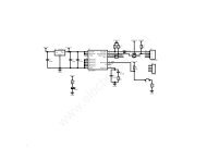
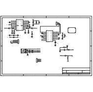
<strong>CC1101</strong>7 Application CircuitOnly a few external components are requiredfor using the <strong>CC1101</strong>. The recommendedapplication circuits are shown in Figure 3 andFigure 4. The external components aredescribed in Table 14, and typical values aregiven in Table 15.Bias Resis<strong>to</strong>rThe bias resis<strong>to</strong>r R171 is used <strong>to</strong> set anaccurate bias current.Balun and RF MatchingThe components between the RF_N/RF_Ppins and the point w<strong>here</strong> the two signals arejoined <strong>to</strong><strong>get</strong>her (C131, C121, L121 and L131for the 315/433 MHz reference design [5].L121, L131, C121, L122, C131, C122 andL132 for the 868/915 MHz reference design[6]) form a balun that converts the differentialRF signal on <strong>CC1101</strong> <strong>to</strong> a single-ended RFsignal. C124 is needed for DC blocking.To<strong>get</strong>her with an appropriate LC network, thebalun components also transform theimpedance <strong>to</strong> match a 50 Ω antenna (orcable). Suggested values for 315 MHz, 433MHz, and 868/915 MHz are listed in Table 15.The balun and LC filter component values andtheir placement are important <strong>to</strong> keep theperformance optimized. It is highlyrecommended <strong>to</strong> follow the <strong>CC1101</strong>EMreference design [5] and [6].CrystalThe crystal oscilla<strong>to</strong>r uses an external crystalwith two loading capaci<strong>to</strong>rs (C81 and C101).See Section 27 on page 53 for details.Additional FilteringAdditional external components (e.g. an RFSAW filter) may be used in order <strong>to</strong> improvethe performance in specific applications.Power Supply DecouplingThe power supply must be properly decoupledclose <strong>to</strong> the supply pins. Note that decouplingcapaci<strong>to</strong>rs are not shown in the applicationcircuit. The placement and the size <strong>of</strong> thedecoupling capaci<strong>to</strong>rs are very important <strong>to</strong>achieve the optimum performance. The<strong>CC1101</strong>EM reference design ([5] and [6])should be followed closely.ComponentC51C81/C101C121/C131C122C123C124C125C126C127L121/L131L122L123L124L125L132R171XTALDescriptionDecoupling capaci<strong>to</strong>r for on-chip voltage regula<strong>to</strong>r <strong>to</strong> digital partCrystal loading capaci<strong>to</strong>rs, see Section 27 on page 53 for detailsRF balun/matching capaci<strong>to</strong>rsRF LC filter/matching filter capaci<strong>to</strong>r (315 and 433 MHz). RF balun/matching capaci<strong>to</strong>r (868/915 MHz).RF LC filter/matching capaci<strong>to</strong>rRF balun DC blocking capaci<strong>to</strong>rRF LC filter DC blocking capaci<strong>to</strong>r (only needed if t<strong>here</strong> is a DC path in the antenna)RF LC filter/matching capaci<strong>to</strong>r/DC-block (868/915 MHz)RF LC filter/matching capaci<strong>to</strong>r (868/915 MHz)RF balun/matching induc<strong>to</strong>rs (inexpensive multi-layer type)RF LC filter/matching filter induc<strong>to</strong>r (315 and 433 MHz). RF balun/matching induc<strong>to</strong>r (868/915 MHz).(inexpensive multi-layer type)RF LC filter/matching filter induc<strong>to</strong>r (inexpensive multi-layer type)RF LC filter/matching filter induc<strong>to</strong>r (inexpensive multi-layer type)RF LC filter/matching filter induc<strong>to</strong>r (inexpensive multi-layer type) (868/915 MHz)RF balun/matching induc<strong>to</strong>r. (inexpensive multi-layer type)Resis<strong>to</strong>r for internal bias current reference.26MHz - 27MHz crystal, see Section 27 on page 53 for details.SWRS061C Page 18 <strong>of</strong> 94
<strong>CC1101</strong>Table 14: Overview <strong>of</strong> External Components (excluding supply decoupling capaci<strong>to</strong>rs)1.8V-3.6V power supplyR171SIDigital IntefaceSCLKSO(GDO1)GDO2(optional)C511 SCLK2 SO(GDO1)3 GDO24 DVDD5 DCOUPLSI 206 GDO0GND 197 CSnDGUARD 188 XOSC_Q1RBIAS 17<strong>CC1101</strong>DIE ATTACH PAD:9 AVDDGND 1610 XOSC_Q2AVDD 15AVDD 14RF_N 13RF_P 12AVDD 11C131L131C121L121C124L122L123C122C125C123Antenna(50 Ohm)GDO0(optional)CSnXTALC81C101Figure 3: Typical Application and Evaluation Circuit 315/433 MHz (excluding supplydecoupling capaci<strong>to</strong>rs)Digital Interface6 GDO07 CSn8 XOSC_Q19 AVDD10 XOSC_Q2SI 20GND 19DGUARD 18RBIAS 17GND 16Figure 4: Typical Application and Evaluation Circuit 868/915 MHz (excluding supplydecoupling capaci<strong>to</strong>rs)SWRS061C Page 19 <strong>of</strong> 94
<strong>CC1101</strong>Component Value at 315MHz Value at 433MHz Value at868/915MHzManufacturerC51 100 nF ± 10%, 0402 X5R Murata GRM1555C seriesC81 27 pF ± 5%, 0402 NP0 Murata GRM1555C seriesC101 27 pF ± 5%, 0402 NP0 Murata GRM1555C seriesC1216.8 pF ± 0.5 pF,0402 NP03.9 pF ± 0.25 pF,0402 NP01.0 pF ± 0.25 pF,0402 NP0Murata GRM1555C seriesC122 12 pF ± 5%, 0402NP08.2 pF ± 0.5 pF,0402 NP01.5 pF ± 0.25 pF,0402 NP0Murata GRM1555C seriesC1236.8 pF ± 0.5 pF,0402 NP05.6 pF ± 0.5 pF,0402 NP03.3 pF ± 0.25 pF,0402 NP0Murata GRM1555C seriesC124 220 pF ± 5%,0402 NP0220 pF ± 5%,0402 NP0100 pF ± 5%, 0402NP0Murata GRM1555C seriesC125 220 pF ± 5%,0402 NP0220 pF ± 5%,0402 NP0100 pF ± 5%, 0402NP0Murata GRM1555C seriesC126 2.2 pF ± 0.25%,0402 NP0C127 2.2 pF ± 0.25%,0402 NP0Murata GRM1555C seriesMurata GRM1555C seriesC1316.8 pF ± 0.5 pF,0402 NP03.9 pF ± 0.25 pF,0402 NP01.5 pF ± 0.25 pF,0402 NP0Murata GRM1555C seriesL121 33 nH ± 5%, 0402monolithic27 nH ± 5%, 0402monolithic12 nH ± 5%, 0402monolithicMurata LQG15HS seriesL122 18 nH ± 5%, 0402monolithic22 nH ± 5%, 0402monolithic18 nH ± 5%, 0402monolithicMurata LQG15HS seriesL123 33 nH ± 5%, 0402monolithic27 nH ± 5%, 0402monolithic12 nH ± 5%, 0402monolithicMurata LQG15HS seriesL124 12 nH ± 5%, 0402monolithicL125 9.1 nH ± 5%, 0402monolithicMurata LQG15HS seriesMurata LQG15HS seriesL131 33 nH ± 5%, 0402monolithic27 nH ± 5%, 0402monolithic12 nH ± 5%, 0402monolithicMurata LQG15HS seriesL132 18 nH ± 5%, 0402monolithicMurata LQG15HS seriesR171 56 kΩ ± 1%, 0402 Koa RK73 seriesXTAL 26.0 MHz surface mount crystal NDK, AT-41CD2Table 15: Bill Of Materials for the Application CircuitThe Gerber files for the <strong>CC1101</strong>EM reference designs ( [5] and [6]) are available from the TI website.SWRS061C Page 20 <strong>of</strong> 94
<strong>CC1101</strong>Default state when the radio is notreceiving or transmitting. Typ.current consumption: 1.7 mA.SIDLESPWD or wake-on-radio (WOR)IDLECSn = 0SXOFFUsed for calibrating frequencySCALsynthesizer upfront (enteringCSn = 0receive or transmit mode can Manual freq.then be done quicker). synth. calibration SRX or STX or SFSTXON or wake-on-radio (WOR)Transitional state. Typ. currentconsumption: 8.4 mA.SleepCrystaloscilla<strong>to</strong>r <strong>of</strong>fLowest power mode. Mostregister values are retained.Current consumption typ400 nA, or typ 900 nA whenwake-on-radio (WOR) isenabled.All register values areretained. Typ. currentconsumption; 165 µA.Frequency synthesizer is on,ready <strong>to</strong> start transmitting.Transmission starts veryquickly after receiving the STXcommand strobe.Typ. currentconsumption: 8.4 mA.Frequencysynthesizer onSFSTXONFrequencysynthesizer startup,optional calibration,settlingSTXFrequency synthesizer is turned on, can optionally becalibrated, and then settles <strong>to</strong> the correct frequency.Transitional state. Typ. current consumption: 8.4 mA.SRX or wake-on-radio (WOR)STXTXOFF_MODE = 01SFSTXON or RXOFF_MODE = 01Typ. current consumption:13.1 mA at -6 dBm output,16.8 mA at 0 dBm output,32.8 mA at +10 dBm output.Transmit modeSTX or RXOFF_MODE=10SRX or TXOFF_MODE = 11Receive modeTyp. currentconsumption:from 14.7 mA (stronginput signal) <strong>to</strong> 15.7 mA(weak input signal).In FIFO-based modes,transmission is turned <strong>of</strong>f andthis state entered if the TXFIFO becomes empty in themiddle <strong>of</strong> a packet. Typ.current consumption: 1.7 mA.TXOFF_MODE = 00RXOFF_MODE = 00Optional transitional state. Typ.current consumption: 8.4 mA.TX FIFOunderflowOptional freq.synth. calibrationRX FIFOoverflowIn FIFO-based modes,reception is turned <strong>of</strong>f and thisstate entered if the RX FIFOoverflows. Typ. currentconsumption: 1.7 mA.SFTXSFRXIDLEFigure 5: Simplified State Diagram, with Typical Current Consumption at 1.2 kBaud Data Rateand MDMCFG2.DEM_DCFILT_OFF=1 (current optimized). Freq. Band = 868 MHzSWRS061C Page 22 <strong>of</strong> 94
<strong>CC1101</strong>9 Configuration S<strong>of</strong>tware<strong>CC1101</strong> can be configured using the SmartRF ®Studio s<strong>of</strong>tware [7]. The SmartRF ® Studios<strong>of</strong>tware is highly recommended for obtainingoptimum register settings, and for evaluatingperformance and functionality. A screenshot <strong>of</strong>the SmartRF ® Studio user interface for <strong>CC1101</strong>is shown in Figure 6.After chip reset, all the registers have defaultvalues as shown in the tables in Section 33.The optimum register setting might differ fromthe default value. After a reset all registers thatshall be different from the default valuet<strong>here</strong>fore needs <strong>to</strong> be programmed throughthe SPI interface.Figure 6: SmartRF ® Studio [7] User Interface10 4-wire Serial Configuration and Data Interface<strong>CC1101</strong> is configured via a simple 4-wire SPIcompatibleinterface (SI, SO, SCLK and CSn)w<strong>here</strong> <strong>CC1101</strong> is the slave. This interface isalso used <strong>to</strong> read and write buffered data. Alltransfers on the SPI interface are done mostsignificant bit first.All transactions on the SPI interface start witha header byte containing a R/W¯ bit, a burstaccess bit (B), and a 6-bit address (A 5 – A 0 ).The CSn pin must be kept low during transferson the SPI bus. If CSn goes high during thetransfer <strong>of</strong> a header byte or during read/writefrom/<strong>to</strong> a register, the transfer will becancelled. The timing for the address and datatransfer on the SPI interface is shown in Figure7 with reference <strong>to</strong> Table 16.When CSn is pulled low, the MCU must waituntil <strong>CC1101</strong> SO pin goes low before starting <strong>to</strong>SWRS061C Page 23 <strong>of</strong> 94
<strong>CC1101</strong>transfer the header byte. This indicates thatthe crystal is running. Unless the chip was inthe SLEEP or XOFF states, the SO pin willalways go low immediately after taking CSnlow.Figure 7: Configuration Registers Write and Read OperationsParameter Description Min Max Unitsf SCLKSCLK frequency100 ns delay inserted between address byte and data byte (single access), orbetween address and data, and between each data byte (burst access).- 10MHzSCLK frequency, single accessNo delay between address and data byte- 9SCLK frequency, burst accessNo delay between address and data byte, or between data bytes- 6.5t sp,pd CSn low <strong>to</strong> positive edge on SCLK, in power-down mode 150 - µst sp CSn low <strong>to</strong> positive edge on SCLK, in active mode 20 - nst ch Clock high 50 - nst cl Clock low 50 - nst rise Clock rise time - 5 nst fall Clock fall time - 5 nst sdSetup data (negative SCLK edge) <strong>to</strong>positive edge on SCLK(t sd applies between address and data bytes, and betweendata bytes)Single accessBurst access5576--nst hd Hold data after positive edge on SCLK 20 - nst ns Negative edge on SCLK <strong>to</strong> CSn high. 20 - nsTable 16: SPI Interface Timing RequirementsNote: The minimum t sp,pd figure in Table 16 can be used in cases w<strong>here</strong> the user does not read theCHIP_RDYn signal. CSn low <strong>to</strong> positive edge on SCLK when the chip is woken from power-downdepends on the start-up time <strong>of</strong> the crystal being used. The 150 us in Table 16 is the crystal oscilla<strong>to</strong>rstart-up time measured on <strong>CC1101</strong>EM reference designs ( [5] and [6]) using crystal AT-41CD2 fromNDK.SWRS061C Page 24 <strong>of</strong> 94
<strong>CC1101</strong>10.1 Chip Status ByteWhen the header byte, data byte, or commandstrobe is sent on the SPI interface, the chipstatus byte is sent by the <strong>CC1101</strong> on the SO pin.The status byte contains key status signals,useful for the MCU. The first bit, s7, is theCHIP_RDYn signal; this signal must go lowbefore the first positive edge <strong>of</strong> SCLK. TheCHIP_RDYn signal indicates that the crystal isrunning.Bits 6, 5, and 4 comprise the STATE value.This value reflects the state <strong>of</strong> the chip. TheXOSC and power <strong>to</strong> the digital core is on inthe IDLE state, but all other modules are inpower down. The frequency and channelconfiguration should only be updated when thechip is in this state. The RX state will be activewhen the chip is in receive mode. Likewise, TXis active when the chip is transmitting.The last four bits (3:0) in the status byte containsFIFO_BYTES_AVAILABLE. For readoperations (the R/W¯ bit in the header byte isset <strong>to</strong> 1), the FIFO_BYTES_AVAILABLE fieldcontains the number <strong>of</strong> bytes available forreading from the RX FIFO. For writeoperations (the R/W¯ bit in the header byte isset <strong>to</strong> 0), the FIFO_BYTES_AVAILABLE fieldcontains the number <strong>of</strong> bytes that can bewritten <strong>to</strong> the TX FIFO. WhenFIFO_BYTES_AVAILABLE=15, 15 or morebytes are available/free.Table 17 gives a status byte summary.Bits Name Description7 CHIP_RDYn Stays high until power and crystal have stabilized. Should always be low when usingthe SPI interface.6:4 STATE[2:0] Indicates the current main state machine modeValue State Description000 IDLE IDLE state(Also reported for some transitional states instead<strong>of</strong> SETTLING or CALIBRATE)001 RX Receive mode010 TX Transmit mode011 FSTXON Fast TX ready100 CALIBRATE Frequency synthesizer calibration is running101 SETTLING PLL is settling110 RXFIFO_OVERFLOW RX FIFO has overflowed. Read out anyuseful data, then flush the FIFO with SFRX111 TXFIFO_UNDERFLOW TX FIFO has underflowed. Acknowledge withSFTX3:0 FIFO_BYTES_AVAILABLE[3:0] The number <strong>of</strong> bytes available in the RX FIFO or free bytes in the TX FIFOTable 17: Status Byte Summary10.2 Register AccessThe configuration registers on the <strong>CC1101</strong> arelocated on SPI addresses from 0x00 <strong>to</strong> 0x2E.Table 35 on page 61 lists all configurationregisters. It is highly recommended <strong>to</strong> useSmartRF ® Studio [7] <strong>to</strong> generate optimumregister settings. The detailed description <strong>of</strong>each register is found in Section 33.1 and33.2, starting on page 64. All configurationregisters can be both written <strong>to</strong> and read. TheR/W¯ bit controls if the register should bewritten <strong>to</strong> or read. When writing <strong>to</strong> registers,the status byte is sent on the SO pin each timea header byte or data byte is transmitted onthe SI pin. When reading from registers, thestatus byte is sent on the SO pin each time aheader byte is transmitted on the SI pin.Registers with consecutive addresses can beaccessed in an efficient way by setting theburst bit (B) in the header byte. The addressbits (A 5 – A 0 ) set the start address in aninternal address counter. This counter isSWRS061C Page 25 <strong>of</strong> 94
<strong>CC1101</strong>incremented by one each new byte (every 8clock pulses). The burst access is either aread or a write access and must be terminatedby setting CSn high.For register addresses in the range 0x30-0x3D, the burst bit is used <strong>to</strong> select betweenstatus registers, burst bit is one, and commandstrobes, burst bit is zero (see 10.4 below).Because <strong>of</strong> this, burst access is not availablefor status registers and they must be accessesone at a time. The status registers can only beread.10.3 SPI ReadWhen reading register fields over the SPIinterface while the register fields are updatedby the radio hardware (e.g. MARCSTATE orTXBYTES), t<strong>here</strong> is a small, but finite,probability that a single read from the registeris being corrupt. As an example, theprobability <strong>of</strong> any single read from TXBYTESbeing corrupt, assuming the maximum datarate is used, is approximately 80 ppm. Refer <strong>to</strong>the <strong>CC1101</strong> Errata Notes [1] for more details.10.4 Command StrobesCommand Strobes may be viewed as singlebyte instructions <strong>to</strong> <strong>CC1101</strong>. By addressing acommand strobe register, internal sequenceswill be started. These commands are used <strong>to</strong>disable the crystal oscilla<strong>to</strong>r, enable receivemode, enable wake-on-radio etc. The 13command strobes are listed in Table 34 onpage 60.The command strobe registers are accessedby transferring a single header byte (no data isbeing transferred). That is, only the R/W¯ bit,the burst access bit (set <strong>to</strong> 0), and the sixaddress bits (in the range 0x30 through 0x3D)are written. The R/W¯ bit can be either one orzero and will determine how theFIFO_BYTES_AVAILABLE field in the statusbyte should be interpreted.When writing command strobes, the statusbyte is sent on the SO pin.A command strobe may be followed by anyother SPI access without pulling CSn high.However, if an SRES strobe is being issued,one will have <strong>to</strong> waith for SO <strong>to</strong> go low againbefore the next header byte can be issued asshown in Figure 8. The command strobes areexecuted immediately, with the exception <strong>of</strong>the SPWD and the SXOFF strobes that areexecuted when CSn goes high.Figure 8: SRES Command Strobe10.5 FIFO AccessThe 64-byte TX FIFO and the 64-byte RXFIFO are accessed through the 0x3F address.When the R/W¯ bit is zero, the TX FIFO isaccessed, and the RX FIFO is accessed whenthe R/W¯ bit is one.The TX FIFO is write-only, while the RX FIFOis read-only.The burst bit is used <strong>to</strong> determine if the FIFOaccess is a single byte access or a burstaccess. The single byte access methodexpects a header byte with the burst bit set <strong>to</strong>zero and one data byte. After the data byte anew header byte is expected; hence, CSn canremain low. The burst access method expectsone header byte and then consecutive databytes until terminating the access by settingCSn high.The following header bytes access the FIFOs:• 0x3F: Single byte access <strong>to</strong> TX FIFO• 0x7F: Burst access <strong>to</strong> TX FIFO• 0xBF: Single byte access <strong>to</strong> RX FIFO• 0xFF: Burst access <strong>to</strong> RX FIFOWhen writing <strong>to</strong> the TX FIFO, the status byte(see Section 10.1) is output for each new databyte on SO, as shown in Figure 7. This statusbyte can be used <strong>to</strong> detect TX FIFO underflowwhile writing data <strong>to</strong> the TX FIFO. Note thatthe status byte contains the number <strong>of</strong> bytesfree before writing the byte in progress <strong>to</strong> theTX FIFO. When the last byte that fits in the TXFIFO is transmitted on SI, the status bytereceived concurrently on SO will indicate tha<strong>to</strong>ne byte is free in the TX FIFO.The TX FIFO may be flushed by issuing aSFTX command strobe. Similarly, a SFRXcommand strobe will flush the RX FIFO. ASFTX or SFRX command strobe can only beissued in the IDLE, TXFIFO_UNDERLOW, orRXFIFO_OVERFLOW states. Both FIFOs areflushed when going <strong>to</strong> the SLEEP state.SWRS061C Page 26 <strong>of</strong> 94
<strong>CC1101</strong>Figure 9 gives a brief overview <strong>of</strong> differentregister access types possible.10.6 PATABLE AccessThe 0x3E address is used <strong>to</strong> access thePATABLE, which is used for selecting PApower control settings. The SPI expects up <strong>to</strong>eight data bytes after receiving the address.By programming the PATABLE, controlled PApower ramp-up and ramp-down can beachieved, as well as ASK modulation shapingfor reduced bandwidth. See SmartRF ® Studio[7] for recommended shaping / PA rampingsequences.See Section 24 on page 49 for details onoutput power programming.The PATABLE is an 8-byte table that definesthe PA control settings <strong>to</strong> use for each <strong>of</strong> theeight PA power values (selected by the 3-bitvalue FREND0.PA_POWER). The table iswritten and read from the lowest setting (0) <strong>to</strong>the highest (7), one byte at a time. An indexcounter is used <strong>to</strong> control the access <strong>to</strong> thetable. This counter is incremented each time abyte is read or written <strong>to</strong> the table, and set <strong>to</strong>the lowest index when CSn is high. When thehighest value is reached the counter restartsat zero.The access <strong>to</strong> the PATABLE is either singlebyte or burst access depending on the burstbit. When using burst access the index counterwill count up; when reaching 7 the counter willrestart at 0. The R/W¯ bit controls whether theaccess is a read or a write access.If one byte is written <strong>to</strong> the PATABLE and thisvalue is <strong>to</strong> be read out then CSn must be sethigh before the read access in order <strong>to</strong> set theindex counter back <strong>to</strong> zero.Note that the content <strong>of</strong> the PATABLE is lostwhen entering the SLEEP state, except for thefirst byte (index 0).Figure 9: Register Access Types11 Microcontroller Interface and Pin ConfigurationIn a typical system, <strong>CC1101</strong> will interface <strong>to</strong> amicrocontroller. This microcontroller must beable <strong>to</strong>:• Program <strong>CC1101</strong> in<strong>to</strong> different modes• Read and write buffered data• Read back status information via the 4-wireSPI-bus configuration interface (SI, SO,SCLK and CSn).11.1 Configuration InterfaceThe microcontroller uses four I/O pins for theSPI configuration interface (SI, SO, SCLK andCSn). The SPI is described in Section 10 onpage 23.11.2 General Control and Status PinsThe <strong>CC1101</strong> has two dedicated configurablepins (GDO0 and GDO2) and one shared pin(GDO1) that can output internal statusinformation useful for control s<strong>of</strong>tware. Thesepins can be used <strong>to</strong> generate interrupts on theMCU. See Section 30 page 55 for more detailson the signals that can be programmed.GDO1 is shared with the SO pin in the SPIinterface. The default setting for GDO1/SO is3-state output. By selecting any other <strong>of</strong> theprogramming options, the GDO1/SO pin willbecome a generic pin. When CSn is low, thepin will always function as a normal SO pin.In the synchronous and asynchronous serialmodes, the GDO0 pin is used as a serial TXdata input pin while in transmit mode.SWRS061C Page 27 <strong>of</strong> 94
<strong>CC1101</strong>The GDO0 pin can also be used for an on-chipanalog temperature sensor. By measuring thevoltage on the GDO0 pin with an externalADC, the temperature can be calculated.Specifications for the temperature sensor arefound in Section 4.7 on page 15.With default PTEST register setting (0x7F) thetemperature sensor output is only availablewhen the frequency synthesizer is enabled(e.g. the MANCAL, FSTXON, RX, and TXstates). It is necessary <strong>to</strong> write 0xBF <strong>to</strong> thePTEST register <strong>to</strong> use the analog temperaturesensor in the IDLE state. Before leaving theIDLE state, the PTEST register should beres<strong>to</strong>red <strong>to</strong> its default value (0x7F).11.3 Optional Radio Control FeatureThe <strong>CC1101</strong> has an optional way <strong>of</strong> controllingthe radio, by reusing SI, SCLK, and CSn fromthe SPI interface. This feature allows for asimple three-pin control <strong>of</strong> the major states <strong>of</strong>the radio: SLEEP, IDLE, RX, and TX.This optional functionality is enabled with theMCSM0.PIN_CTRL_EN configuration bit.State changes are commanded as follows:When CSn is high the SI and SCLK is set <strong>to</strong>the desired state according <strong>to</strong> Table 18. When12 Data Rate ProgrammingThe data rate used when transmitting, or thedata rate expected in receive is programmedby the MDMCFG3.DRATE_M and theMDMCFG4.DRATE_E configuration registers.The data rate is given by the formula below.As the formula shows, the programmed datarate depends on the crystal frequency.CSn goes low the state <strong>of</strong> SI and SCLK islatched and a command strobe is generatedinternally according <strong>to</strong> the pin configuration. Itis only possible <strong>to</strong> change state with thisfunctionality. That means that for instance RXwill not be restarted if SI and SCLK are set <strong>to</strong>RX and CSn <strong>to</strong>ggles. When CSn is low the SIand SCLK has normal SPI functionality.All pin control command strobes are executedimmediately, except the SPWD strobe, which isdelayed until CSn goes high.CSn SCLK SI Function1 X X Chip unaffected by SCLK/SI↓ 0 0 Generates SPWD strobe↓ 0 1 Generates STX strobe↓ 1 0 Generates SIDLE strobe↓ 1 1 Generates SRX strobe0SPImodeSPImodeSPI mode (wakes up in<strong>to</strong>IDLE if in SLEEP/XOFF)Table 18: Optional Pin Control CodingIf DRATE_M is rounded <strong>to</strong> the nearest integerand becomes 256, increment DRATE_E anduse DRATE_M = 0.The data rate can be set from 1.2 kBaud <strong>to</strong>500 kBaud with the minimum step size <strong>of</strong>:R( 256 + DRATE _ M )DATA=282⋅ 2DRATE _ E⋅ fXOSCThe following approach can be used <strong>to</strong> findsuitable values for a given data rate:⎢ ⎛ RDRATE _ E = ⎢log2⎜⎢⎣⎝ fDRATE _ M =fRDATA⋅ 2⋅ 2XOSC2028DATADRATE _ EXOSC⋅ 2⎞⎥⎟⎥⎠⎥⎦− 256SWRS061C Page 28 <strong>of</strong> 94
<strong>CC1101</strong>Min DataRate[kBaud]Typical DataRate[kBaud]Max DataRate[kBaud]Data rateStep Size[kBaud]0.8 1.2 / 2.4 3.17 0.00623.17 4.8 6.35 0.01246.35 9.6 12.7 0.024812.7 19.6 25.4 0.049625.4 38.4 50.8 0.0992Min DataRate[kBaud]Typical DataRate[kBaud]Max DataRate[kBaud]Data rateStep Size[kBaud]50.8 76.8 101.6 0.1984101.6 153.6 203.1 0.3967203.1 250 406.3 0.7935406.3 500 500 1.5869Table 19: Data Rate Step SizeSWRS061C Page 29 <strong>of</strong> 94
<strong>CC1101</strong>13 Receiver Channel Filter BandwidthIn order <strong>to</strong> meet different channel widthrequirements, the receiver channel filter isprogrammable. The MDMCFG4.CHANBW_E andMDMCFG4.CHANBW_M configuration registerscontrol the receiver channel filter bandwidth,which scales with the crystal oscilla<strong>to</strong>rfrequency. The following formula gives t<strong>here</strong>lation between the register settings and thechannel filter bandwidth:BWchannelfXOSC=8 ⋅ (4 + CHANBW _ M )·2CHANBW _ EThe <strong>CC1101</strong> supports the following channel filterbandwidths:MDMCFG4.MDMCFG4.CHANBW_ECHANBW_M 00 01 10 1100 812 406 203 10201 650 325 162 81For best performance, the channel filterbandwidth should be selected so that thesignal bandwidth occupies at most 80% <strong>of</strong> thechannel filter bandwidth. The channel centre<strong>to</strong>lerance due <strong>to</strong> crystal accuracy should alsobe subtracted from the signal bandwidth. Thefollowing example illustrates this:With the channel filter bandwidth set <strong>to</strong>500 kHz, the signal should stay within 80% <strong>of</strong>500 kHz, which is 400 kHz. Assuming915 MHz frequency and ±20 ppm frequencyuncertainty for both the transmitting device andthe receiving device, the <strong>to</strong>tal frequencyuncertainty is ±40 ppm <strong>of</strong> 915MHz, which is±37 kHz. If the whole transmitted signalbandwidth is <strong>to</strong> be received within 400kHz, thetransmitted signal bandwidth should bemaximum 400kHz – 2·37 kHz, which is326 kHz.10 541 270 135 6811 464 232 116 58Table 20: Channel Filter Bandwidths [kHz](Assuming a 26MHz crystal)14 Demodula<strong>to</strong>r, Symbol Synchronizer, and Data Decision<strong>CC1101</strong> contains an advanced and highlyconfigurable demodula<strong>to</strong>r. Channel filteringand frequency <strong>of</strong>fset compensation isperformed digitally. To generate the RSSI level(see Section 17.3 for more information) thesignal level in the channel is estimated. Datafiltering is also included for enhancedperformance.14.1 Frequency Offset CompensationWhen using 2-FSK, GFSK, or MSKmodulation, the demodula<strong>to</strong>r will compensatefor the <strong>of</strong>fset between the transmitter andreceiver frequency, within certain limits, byestimating the centre <strong>of</strong> the received data.This value is available in the FREQEST statusregister. Writing the value from FREQEST in<strong>to</strong>FSCTRL0.FREQOFF the frequencysynthesizer is au<strong>to</strong>matically adjustedaccording <strong>to</strong> the estimated frequency <strong>of</strong>fset.The tracking range <strong>of</strong> the algorithm isselectable as fractions <strong>of</strong> the channelbandwidth with the FOCCFG.FOC_LIMITconfiguration register.If the FOCCFG.FOC_BS_CS_GATE bit is set,the <strong>of</strong>fset compensa<strong>to</strong>r will freeze until carriersense asserts. This may be useful when theradio is in RX for long periods with no traffic,since the algorithm may drift <strong>to</strong> the boundarieswhen trying <strong>to</strong> track noise.The tracking loop has two gain fac<strong>to</strong>rs, whichaffects the settling time and noise sensitivity <strong>of</strong>the algorithm. FOCCFG.FOC_PRE_K sets thegain before the sync word is detected, andFOCCFG.FOC_POST_K selects the gain afterthe sync word has been found.Note that frequency <strong>of</strong>fset compensation is notsupported for ASK or OOK modulation.14.2 Bit SynchronizationThe bit synchronization algorithm extracts theclock from the incoming symbols. Thealgorithm requires that the expected data rateis programmed as described in Section 12 onpage 28. Re-synchronization is performedcontinuously <strong>to</strong> adjust for error in the incomingsymbol rate.SWRS061C Page 30 <strong>of</strong> 94
<strong>CC1101</strong>14.3 Byte SynchronizationByte synchronization is achieved by acontinuous sync word search. The sync wordis a 16 bit configurable field (can be repeated<strong>to</strong> <strong>get</strong> a 32 bit) that is au<strong>to</strong>matically inserted atthe start <strong>of</strong> the packet by the modula<strong>to</strong>r intransmit mode. The demodula<strong>to</strong>r uses thisfield <strong>to</strong> find the byte boundaries in the stream<strong>of</strong> bits. The sync word will also function as asystem identifier, since only packets with thecorrect predefined sync word will be received ifthe sync word detection in RX is enabled inregister MDMCFG2 (see Section 17.1).. Thesync word detec<strong>to</strong>r correlates against theuser-configured 16 or 32 bit sync word. Thecorrelation threshold can be set <strong>to</strong> 15/16,15 Packet Handling Hardware SupportThe <strong>CC1101</strong> has built-in hardware support forpacket oriented radio pro<strong>to</strong>cols.In transmit mode, the packet handler can beconfigured <strong>to</strong> add the following elements <strong>to</strong> thepacket s<strong>to</strong>red in the TX FIFO:• A programmable number <strong>of</strong> preamblebytes• A two byte synchronization (sync) word.Can be duplicated <strong>to</strong> give a 4-byte syncword (recommended). It is not possible <strong>to</strong>only insert preamble or only insert a syncword.• A CRC checksum computed over the datafield.The recommended setting is 4-byte preambleand 4-byte sync word, except for 500 kBauddata rate w<strong>here</strong> the recommended preamblelength is 8 bytes.In addition, the following can be implementedon the data field and the optional 2-byte CRCchecksum:• Whitening <strong>of</strong> the data with a PN9sequence.• Forward error correction by the use <strong>of</strong>interleaving and coding <strong>of</strong> the data(convolutional coding).In receive mode, the packet handling supportwill de-construct the data packet byimplementing the following (if enabled):• Preamble detection.• Sync word detection.16/16, or 30/32 bits match. The sync word canbe further qualified using the preamble qualityindica<strong>to</strong>r mechanism described below and/or acarrier sense condition. The sync word isconfigured through the SYNC1 and SYNC0registers.In order <strong>to</strong> make false detections <strong>of</strong> syncwords less likely, a mechanism calledpreamble quality indication (PQI) can be used<strong>to</strong> qualify the sync word. A threshold value forthe preamble quality must be exceeded inorder for a detected sync word <strong>to</strong> be accepted.See Section 17.2 on page 37 for more details.• CRC computation and CRC check.• One byte address check.• Packet length check (length byte checkedagainst a programmable maximumlength).• De-whitening• De-interleaving and decodingOptionally, two status bytes (see Table 21 andTable 22) with RSSI value, Link QualityIndication, and CRC status can be appendedin the RX FIFO.Bit Field Name Description7:0 RSSI RSSI valueTable 21: Received Packet Status Byte 1(first byte appended after the data)Bit Field Name Description7 CRC_OK 1: CRC for received data OK(or CRC disabled)0: CRC error in received data6:0 LQI Indicating the link qualityTable 22: Received Packet Status Byte 2(second byte appended after the data)Note that register fields that control the packethandling features should only be altered when<strong>CC1101</strong> is in the IDLE state.SWRS061C Page 31 <strong>of</strong> 94
<strong>CC1101</strong>15.1 Data WhiteningFrom a radio perspective, the ideal over the airdata are random and DC free. This results inthe smoothest power distribution over theoccupied bandwidth. This also gives t<strong>here</strong>gulation loops in the receiver uniformoperation conditions (no data dependencies).Real world data <strong>of</strong>ten contain long sequences<strong>of</strong> zeros and ones. Performance can then beimproved by whitening the data beforetransmitting, and de-whitening the data in t<strong>here</strong>ceiver. With <strong>CC1101</strong>, this can be doneau<strong>to</strong>matically by settingPKTCTRL0.WHITE_DATA=1. All data, exceptthe preamble and the sync word, are thenXOR-ed with a 9-bit pseudo-random (PN9)sequence before being transmitted, as shownin Figure 10. At the receiver end, the data areXOR-ed with the same pseudo-randomsequence. This way, the whitening is reversed,and the original data appear in the receiver.The PN9 sequence is initialized <strong>to</strong> all 1’s.Figure 10: Data Whitening in TX Mode15.2 Packet FormatThe format <strong>of</strong> the data packet can beconfigured and consists <strong>of</strong> the following items(see Figure 11):• Preamble• Synchronization word• Optional length byte• Optional address byte• Payload• Optional 2 byte CRC•Optional data whiteningOptionally FEC encoded/decodedOptional CRC-16 calculationLegend:Inserted au<strong>to</strong>matically in TX,processed and removed in RX.Preamble bits(1010...1010)Sync word8 x n bits 16/32 bitsLength field8bitsAddress field8bitsData fieldCRC-168 x n bits 16 bitsOptional user-provided fields processed in TX,processed but not removed in RX.Unprocessed user data (apart from FECand/or whitening)Figure 11: Packet FormatSWRS061C Page 32 <strong>of</strong> 94
<strong>CC1101</strong>The preamble pattern is an alternatingsequence <strong>of</strong> ones and zeros (10101010…).The minimum length <strong>of</strong> the preamble isprogrammable. When enabling TX, themodula<strong>to</strong>r will start transmitting the preamble.When the programmed number <strong>of</strong> preamblebytes has been transmitted, the modula<strong>to</strong>r willsend the sync word and then data from the TXFIFO if data is available. If the TX FIFO isempty, the modula<strong>to</strong>r will continue <strong>to</strong> sendpreamble bytes until the first byte is written <strong>to</strong>the TX FIFO. The modula<strong>to</strong>r will then send thesync word and then the data bytes. Thenumber <strong>of</strong> preamble bytes is programmed withthe MDMCFG1.NUM_PREAMBLE value.The synchronization word is a two-byte valueset in the SYNC1 and SYNC0 registers. Thesync word provides byte synchronization <strong>of</strong> theincoming packet. A one-byte synch word canbe emulated by setting the SYNC1 value <strong>to</strong> thepreamble pattern. It is also possible <strong>to</strong> emulatea 32 bit sync word by usingMDMCFG2.SYNC_MODE set <strong>to</strong> 3 or 7. The syncword will then be repeated twice.<strong>CC1101</strong> supports both constant packet lengthpro<strong>to</strong>cols and variable length pro<strong>to</strong>cols.Variable or fixed packet length mode can beused for packets up <strong>to</strong> 255 bytes. For longerpackets, infinite packet length mode must beused.Fixed packet length mode is selected bysetting PKTCTRL0.LENGTH_CONFIG=0. Thedesired packet length is set by the PKTLENregister.In variable packet length mode,PKTCTRL0.LENGTH_CONFIG=1, the packetlength is configured by the first byte after thesync word. The packet length is defined as thepayload data, excluding the length byte andthe optional CRC. The PKTLEN register isused <strong>to</strong> set the maximum packet lengthallowed in RX. Any packet received with alength byte with a value greater than PKTLENwill be discarded.With PKTCTRL0.LENGTH_CONFIG=2, thepacket length is set <strong>to</strong> infinite and transmissionand reception will continue until turned <strong>of</strong>fmanually. As described in the next section, thiscan be used <strong>to</strong> support packet formats withdifferent length configuration than nativelysupported by <strong>CC1101</strong>. One should make surethat TX mode is not turned <strong>of</strong>f during thetransmission <strong>of</strong> the first half <strong>of</strong> any byte. Refer<strong>to</strong> the <strong>CC1101</strong> Errata Notes [1] for more details.Note that the minimum packet lengthsupported (excluding the optional length byteand CRC) is one byte <strong>of</strong> payload data.15.2.1 Arbitrary Length Field ConfigurationThe packet length register, PKTLEN, can bereprogrammed during receive and transmit. Incombination with fixed packet length mode(PKTCTRL0.LENGTH_CONFIG=0) this opensthe possibility <strong>to</strong> have a different length fieldconfiguration than supported for variablelength packets (in variable packet length modethe length byte is the first byte after the syncword). At the start <strong>of</strong> reception, the packetlength is set <strong>to</strong> a large value. The MCU readsout enough bytes <strong>to</strong> interpret the length field inthe packet. Then the PKTLEN value is setaccording <strong>to</strong> this value. The end <strong>of</strong> packet willoccur when the byte counter in the packethandler is equal <strong>to</strong> the PKTLEN register. Thus,the MCU must be able <strong>to</strong> program the correctlength, before the internal counter reaches thepacket length.15.2.2 Packet Length > 255Also the packet au<strong>to</strong>mation control register,PKTCTRL0, can be reprogrammed during TXand RX. This opens the possibility <strong>to</strong> transmitand receive packets that are longer than 256bytes and still be able <strong>to</strong> use the packethandling hardware support. At the start <strong>of</strong> thepacket, the infinite packet length mode(PKTCTRL0.LENGTH_CONFIG=2) must beactive. On the TX side, the PKTLEN register isset <strong>to</strong> mod(length, 256). On the RX side theMCU reads out enough bytes <strong>to</strong> interpret thelength field in the packet and sets the PKTLENregister <strong>to</strong> mod(length, 256). When less than256 bytes remains <strong>of</strong> the packet the MCUdisables infinite packet length mode andactivates fixed packet length mode. When theinternal byte counter reaches the PKTLENvalue, the transmission or reception ends (theradio enters the state determined byTXOFF_MODE or RXOFF_MODE). Au<strong>to</strong>maticCRC appending/checking can also be used(by setting PKTCTRL0.CRC_EN=1).When for example a 600-byte packet is <strong>to</strong> betransmitted, the MCU should do the following(see also Figure 12)• Set PKTCTRL0.LENGTH_CONFIG=2.• Pre-program the PKTLEN register <strong>to</strong>mod(600, 256) = 88.SWRS061C Page 33 <strong>of</strong> 94
<strong>CC1101</strong>• Transmit at least 345 bytes (600 - 255), forexample by filling the 64-byte TX FIFO sixtimes (384 bytes transmitted).• Set PKTCTRL0.LENGTH_CONFIG=0.• The transmission ends when the packetcounter reaches 88. A <strong>to</strong>tal <strong>of</strong> 600 bytesare transmitted.Internal byte counter in packet handler counts from 0 <strong>to</strong> 255 and then starts at 0 again0,1,..........,88,....................255,0,........,88,..................,255,0,........,88,..................,255,0,.......................Infinite packet length enabledFixed packet lengthenabled when less than256 bytes remains <strong>of</strong>packet600 bytes transmitted andreceivedLength field transmitted and received. Rx and Tx PKTLEN value set <strong>to</strong> mod(600,256) = 88Figure 12: Packet Length > 25515.3 Packet Filtering in Receive Mode<strong>CC1101</strong> supports three different types <strong>of</strong>packet-filtering; address filtering, maximumlength filtering, and CRC filtering.15.3.1 Address FilteringSetting PKTCTRL1.ADR_CHK <strong>to</strong> any othervalue than zero enables the packet addressfilter. The packet handler engine will comparethe destination address byte in the packet withthe programmed node address in the ADDRregister and the 0x00 broadcast address whenPKTCTRL1.ADR_CHK=10 or both 0x00 and0xFF broadcast addresses whenPKTCTRL1.ADR_CHK=11. If the receivedaddress matches a valid address, the packet isreceived and written in<strong>to</strong> the RX FIFO. If theaddress match fails, the packet is discardedand receive mode restarted (regardless <strong>of</strong> theMCSM1.RXOFF_MODE setting).If the received address matches a validaddress when using infinite packet lengthmode and address filtering is enabled, 0xFFwill be written in<strong>to</strong> the RX FIFO followed by theaddress byte and then the payload data.15.3.2 Maximum Length FilteringIn variable packet length mode,PKTCTRL0.LENGTH_CONFIG=1, thePKTLEN.PACKET_LENGTH register value isused <strong>to</strong> set the maximum allowed packetlength. If the received length byte has a largervalue than this, the packet is discarded andreceive mode restarted (regardless <strong>of</strong> theMCSM1.RXOFF_MODE setting).15.3.3 CRC FilteringThe filtering <strong>of</strong> a packet when CRC check failsis enabled by settingPKTCTRL1.CRC_AUTOFLUSH=1. The CRCau<strong>to</strong> flush function will flush the entire RXFIFO if the CRC check fails. After au<strong>to</strong> flushingthe RX FIFO, the next state depends on theMCSM1.RXOFF_MODE setting.When using the au<strong>to</strong> flush function, themaximum packet length is 63 bytes in variablepacket length mode and 64 bytes in fixedpacket length mode. Note that the maximumallowed packet length is reduced by two byteswhen PKTCTRL1.APPEND_STATUS isenabled, <strong>to</strong> make room in the RX FIFO for thetwo status bytes appended at the end <strong>of</strong> thepacket. Since the entire RX FIFO is flushedwhen the CRC check fails, the previouslyreceived packet must be read out <strong>of</strong> the FIFObefore receiving the current packet. The MCUmust not read from the current packet until theCRC has been checked as OK.15.4 Packet Handling in Transmit ModeThe payload that is <strong>to</strong> be transmitted must bewritten in<strong>to</strong> the TX FIFO. The first byte writtenmust be the length byte when variable packetlength is enabled. The length byte has a valueequal <strong>to</strong> the payload <strong>of</strong> the packet (includingSWRS061C Page 34 <strong>of</strong> 94
<strong>CC1101</strong>the optional address byte). If addressrecognition is enabled on the receiver, thesecond byte written <strong>to</strong> the TX FIFO must bethe address byte. If fixed packet length isenabled, then the first byte written <strong>to</strong> the TXFIFO should be the address (if the receiveruses address recognition).The modula<strong>to</strong>r will first send the programmednumber <strong>of</strong> preamble bytes. If data is availablein the TX FIFO, the modula<strong>to</strong>r will send thetwo-byte (optionally 4-byte) sync word andthen the payload in the TX FIFO. If CRC isenabled, the checksum is calculated over allthe data pulled from the TX FIFO and t<strong>here</strong>sult is sent as two extra bytes following thepayload data. If the TX FIFO runs emptybefore the complete packet has beentransmitted, the radio will enterTXFIFO_UNDERFLOW state. The only way <strong>to</strong>exit this state is by issuing an SFTX strobe.Writing <strong>to</strong> the TX FIFO after it has underflowedwill not restart TX mode.If whitening is enabled, everything followingthe sync words will be whitened. This is donebefore the optional FEC/Interleaver stage.Whitening is enabled by settingPKTCTRL0.WHITE_DATA=1.If FEC/Interleaving is enabled, everythingfollowing the sync words will be scrambled bythe interleaver and FEC encoded before beingmodulated. FEC is enabled by settingMDMCFG1.FEC_EN=1.15.5 Packet Handling in Receive ModeIn receive mode, the demodula<strong>to</strong>r and packethandler will search for a valid preamble andthe sync word. When found, the demodula<strong>to</strong>rhas obtained both bit and byte synchronismand will receive the first payload byte.If FEC/Interleaving is enabled, the FECdecoder will start <strong>to</strong> decode the first payloadbyte. The interleaver will de-scramble the bitsbefore any other processing is done <strong>to</strong> thedata.If whitening is enabled, the data will be dewhitenedat this stage.When variable packet length mode is enabled,the first byte is the length byte. The packethandler s<strong>to</strong>res this value as the packet lengthand receives the number <strong>of</strong> bytes indicated bythe length byte. If fixed packet length mode isused, the packet handler will accept theprogrammed number <strong>of</strong> bytes.Next, the packet handler optionally checks theaddress and only continues the reception if theaddress matches. If au<strong>to</strong>matic CRC check isenabled, the packet handler computes CRCand matches it with the appended CRCchecksum.At the end <strong>of</strong> the payload, the packet handlerwill optionally write two extra packet statusbytes (see Table 21 and Table 22) that containCRC status, link quality indication, and RSSIvalue.15.6 Packet Handling in FirmwareWhen implementing a packet oriented radiopro<strong>to</strong>col in firmware, the MCU needs <strong>to</strong> knowwhen a packet has been received/transmitted.Additionally, for packets longer than 64 bytesthe RX FIFO needs <strong>to</strong> be read while in RX andthe TX FIFO needs <strong>to</strong> be refilled while in TX.This means that the MCU needs <strong>to</strong> know thenumber <strong>of</strong> bytes that can be read from orwritten <strong>to</strong> the RX FIFO and TX FIFOrespectively. T<strong>here</strong> are two possible solutions<strong>to</strong> <strong>get</strong> the necessary status information:a) Interrupt Driven SolutionIn both RX and TX one can use one <strong>of</strong> theGDO pins <strong>to</strong> give an interrupt when a syncword has been received/transmitted and/orwhen a complete packet has beenreceived/transmitted(IOCFGx.GDOx_CFG=0x06). In addition, t<strong>here</strong>are 2 configurations for theIOCFGx.GDOx_CFG register that areassociated with the RX FIFO(IOCFGx.GDOx_CFG=0x00andIOCFGx.GDOx_CFG=0x01) and two that areassociated with the TX FIFO(IOCFGx.GDOx_CFG=0x02andIOCFGx.GDOx_CFG=0x03) that can be usedas interrupt sources <strong>to</strong> provide information onhow many bytes are in the RX FIFO and TXFIFO respectively. See Table 33.b) SPI PollingThe PKTSTATUS register can be polled at agiven rate <strong>to</strong> <strong>get</strong> information about the currentGDO2 and GDO0 values respectively. TheRXBYTES and TXBYTES registers can bepolled at a given rate <strong>to</strong> <strong>get</strong> information aboutthe number <strong>of</strong> bytes in the RX FIFO and TXFIFO respectively. Alternatively, the number <strong>of</strong>bytes in the RX FIFO and TX FIFO can beread from the chip status byte returned on theSWRS061C Page 35 <strong>of</strong> 94
<strong>CC1101</strong>MISO line each time a header byte, data byte,or command strobe is sent on the SPI bus.It is recommended <strong>to</strong> employ an interruptdriven solution as high rate SPI polling willreduce the RX sensitivity. Furthermore, asexplained in Section 10.3 and the <strong>CC1101</strong>Errata Notes [1], when using SPI polling t<strong>here</strong>is a small, but finite, probability that a singleread from registers PKTSTATUS , RXBYTESand TXBYTES is being corrupt. The same isthe case when reading the chip status byte.Refer <strong>to</strong> the TI website for SW examples ([8]and [9]).16 Modulation Formats<strong>CC1101</strong> supports amplitude, frequency, andphase shift modulation formats. The desiredmodulation format is set in theMDMCFG2.MOD_FORMAT register.Optionally, the data stream can be Manchestercoded by the modula<strong>to</strong>r and decoded by thedemodula<strong>to</strong>r. This option is enabled by settingMDMCFG2.MANCHESTER_EN=1. Manchesterencoding is not supported at the same time asusing the FEC/Interleaver option.16.1 Frequency Shift Keying2-FSK can optionally be shaped by aGaussian filter with BT = 1, producing a GFSKmodulated signal.The frequency deviation is programmed withthe DEVIATION_M and DEVIATION_E valuesin the DEVIATN register. The value has anexponent/mantissa form, and the resultantdeviation is given by:fdevf=2xoscDEVIATION _ E⋅ (8 + DEVIATION _ M ) ⋅ 217The symbol encoding is shown in Table 23.Format Symbol Coding2-FSK/GFSK ‘0’ – Deviation‘1’ + DeviationTable 23: Symbol Encoding for 2-FSK/GFSKModulation16.2 Minimum Shift KeyingWhen using MSK 1 , the complete transmission(preamble, sync word, and payload) will beMSK modulated.Phase shifts are performed with a constanttransition time.The fraction <strong>of</strong> a symbol period used <strong>to</strong>change the phase can be modified with theDEVIATN.DEVIATION_M setting. This isequivalent <strong>to</strong> changing the shaping <strong>of</strong> thesymbol.The MSK modulation format implemented in<strong>CC1101</strong> inverts the sync word and datacompared <strong>to</strong> e.g. signal genera<strong>to</strong>rs.16.3 Amplitude Modulation<strong>CC1101</strong> supports two different forms <strong>of</strong>amplitude modulation: On-Off Keying (OOK)and Amplitude Shift Keying (ASK).OOK modulation simply turns on or <strong>of</strong>f the PA<strong>to</strong> modulate 1 and 0 respectively.The ASK variant supported by the <strong>CC1101</strong>allows programming <strong>of</strong> the modulation depth(the difference between 1 and 0), and shaping<strong>of</strong> the pulse amplitude. Pulse shaping willproduce a more bandwidth constrained outputspectrum.1Identical <strong>to</strong> <strong>of</strong>fset QPSK with half-sineshaping (data coding may differ)SWRS061C Page 36 <strong>of</strong> 94
<strong>CC1101</strong>17 Received Signal Qualifiers and Link Quality Information<strong>CC1101</strong> has several qualifiers that can be used<strong>to</strong> increase the likelihood that a valid syncword is detected.17.1 Sync Word QualifierIf sync word detection in RX is enabled inregister MDMCFG2 the <strong>CC1101</strong> will not start fillingthe RX FIFO and perform the packet filteringdescribed in Section 15.3 before a valid syncword has been detected. The sync wordqualifier mode is set by MDMCFG2.SYNC_MODEand is summarized in Table 24. Carrier senseis described in Section 17.4.MDMCFG2.SYNC_MODESync Word Qualifier Mode000 No preamble/sync001 15/16 sync word bits detected010 16/16 sync word bits detected011 30/32 sync word bits detected100 No preamble/sync, carrier senseabove threshold101 15/16 + carrier sense above threshold110 16/16 + carrier sense above threshold111 30/32 + carrier sense above thresholdTable 24: Sync Word Qualifier Mode17.2 Preamble Quality Threshold (PQT)The Preamble Quality Threshold (PQT) syncwordqualifier adds the requirement that t<strong>here</strong>ceived sync word must be preceded with apreamble with a quality above theprogrammed threshold.Another use <strong>of</strong> the preamble quality thresholdis as a qualifier for the optional RX terminationtimer. See Section 19.7 on page 46 for details.The preamble quality estima<strong>to</strong>r increases aninternal counter by one each time a bit isreceived that is different from the previous bit,and decreases the counter by 8 each time abit is received that is the same as the last bit.The threshold is configured with the registerfield PKTCTRL1.PQT. A threshold <strong>of</strong> 4·PQT forthis counter is used <strong>to</strong> gate sync worddetection. By setting the value <strong>to</strong> zero, thepreamble quality qualifier <strong>of</strong> the synch word isdisabled.A “Preamble Quality Reached” signal can beobserved on one <strong>of</strong> the GDO pins by settingIOCFGx.GDOx_CFG=8. It is also possible <strong>to</strong>determine if preamble quality is reached bychecking the PQT_REACHED bit in thePKTSTATUS register. This signal / bit assertswhen the received signal exceeds the PQT.17.3 RSSIThe RSSI value is an estimate <strong>of</strong> the signalpower level in the chosen channel. This valueis based on the current gain setting in the RXchain and the measured signal level in thechannel.In RX mode, the RSSI value can be readcontinuously from the RSSI status register untilthe demodula<strong>to</strong>r detects a sync word (whensync word detection is enabled). At that pointthe RSSI readout value is frozen until the nexttime the chip enters the RX state. The RSSIvalue is in dBm with ½dB resolution. The RSSIupdate rate, f RSSI , depends on the receiverfilter bandwidth (BW channel defined in Section13) and AGCCTRL0.FILTER_LENGTH.fRSSI2 ⋅ BW=8⋅2channelFILTER _ LENGTHIf PKTCTRL1.APPEND_STATUS is enabled thelast RSSI value <strong>of</strong> the packet is au<strong>to</strong>maticallyadded <strong>to</strong> the first byte appended after thepayload.The RSSI value read from the RSSI statusregister is a 2’s complement number. Thefollowing procedure can be used <strong>to</strong> convert theRSSI reading <strong>to</strong> an absolute power level(RSSI_dBm).1) Read the RSSI status register2) Convert the reading from a hexadecimalnumber <strong>to</strong> a decimal number (RSSI_dec)3) If RSSI_dec ≥ 128 then RSSI_dBm =(RSSI_dec - 256)/2 – RSSI_<strong>of</strong>fset4) Else if RSSI_dec < 128 then RSSI_dBm =(RSSI_dec)/2 – RSSI_<strong>of</strong>fsetTable 25 gives typical values for theRSSI_<strong>of</strong>fset.Figure 13 and Figure 14 shows typical plots <strong>of</strong>RSSI reading as a function <strong>of</strong> input powerlevel for different data rates.SWRS061C Page 37 <strong>of</strong> 94
<strong>CC1101</strong>Data rate [kBaud] RSSI_<strong>of</strong>fset [dB], 433 MHz RSSI_<strong>of</strong>fset [dB], 868 MHz1.2 74 7438.4 74 74250 74 74500 74 74Table 25: Typical RSSI_<strong>of</strong>fset Values0-10-20-30RSSI Readout [dBm]-40-50-60-70-80-90-100-110-120-120 -110 -100 -90 -80 -70 -60 -50 -40 -30 -20 -10 0Input Power [dBm]1.2 kBaud 38.4 kBaud 250 kBaud 500 kBaudFigure 13: Typical RSSI Value vs. Input Power Level for Different Data Rates at 433 MHz0-10-20-30RSSI Readout [dBm]-40-50-60-70-80-90-100-110-120-120 -110 -100 -90 -80 -70 -60 -50 -40 -30 -20 -10 0Input Power [dBm]1.2 kBaud 38.4 kBaud 250 kBaud 500 kBaudFigure 14: Typical RSSI Value vs. Input Power Level for Different Data Rates at 868 MHzSWRS061C Page 38 <strong>of</strong> 94
<strong>CC1101</strong>17.4 Carrier Sense (CS)Carrier Sense (CS) is used as a sync wordqualifier and for CCA and can be assertedbased on two conditions, which can beindividually adjusted:• CS is asserted when the RSSI is above aprogrammable absolute threshold, and deassertedwhen RSSI is below the samethreshold (with hysteresis).• CS is asserted when the RSSI hasincreased with a programmable number <strong>of</strong>dB from one RSSI sample <strong>to</strong> the next, andde-asserted when RSSI has decreasedwith the same number <strong>of</strong> dB. This settingis not dependent on the absolute signallevel and is thus useful <strong>to</strong> detect signals inenvironments with time varying noise floor.Carrier Sense can be used as a sync wordqualifier that requires the signal level <strong>to</strong> behigher than the threshold for a sync wordsearch <strong>to</strong> be performed. The signal can alsobe observed on one <strong>of</strong> the GDO pins bysetting IOCFGx.GDOx_CFG=14 and in thestatus register bit PKTSTATUS.CS.Other uses <strong>of</strong> Carrier Sense include the TX-if-CCA function (see Section 17.5 on page 40)and the optional fast RX termination (seeSection 19.7 on page 46).CS can be used <strong>to</strong> avoid interference fromother RF sources in the ISM bands.17.4.1 CS Absolute ThresholdThe absolute threshold related <strong>to</strong> the RSSIvalue depends on the following register fields:• AGCCTRL2.MAX_LNA_GAIN• AGCCTRL2.MAX_DVGA_GAIN• AGCCTRL1.CARRIER_SENSE_ABS_THR• AGCCTRL2.MAGN_TARGET• For a given AGCCTRL2.MAX_LNA_GAINand AGCCTRL2.MAX_DVGA_GAIN setting theabsolute threshold can be adjusted ±7 dB insteps <strong>of</strong> 1 dB usingCARRIER_SENSE_ABS_THR.The MAGN_TARGET setting is a compromisebetween blocker <strong>to</strong>lerance/selectivity andsensitivity. The value sets the desired signallevel in the channel in<strong>to</strong> the demodula<strong>to</strong>r.Increasing this value reduces the headroomfor blockers, and t<strong>here</strong>fore close-in selectivity.It is strongly recommended <strong>to</strong> use SmartRF ®Studio <strong>to</strong> generate the correct MAGN_TARGETsetting.Table 26 and Table 27 show the typical RSSIreadout values at the CS threshold at 2.4kBaud and 250 kBaud data rate respectively.The default CARRIER_SENSE_ABS_THR=0 (0dB) and MAGN_TARGET=3 (33 dB) have beenused.For other data rates the user must generatesimilar tables <strong>to</strong> find the CS absolutethreshold.MAX_LNA_GAIN[2:0]MAX_DVGA_GAIN[1:0]00 01 10 11000 -97.5 -91.5 -85.5 -79.5001 -94 -88 -82.5 -76010 -90.5 -84.5 -78.5 -72.5011 -88 -82.5 -76.5 -70.5100 -85.5 -80 -73.5 -68101 -84 -78 -72 -66110 -82 -76 -70 -64111 -79 -73.5 -67 -61Table 26: Typical RSSI Value in dBm at CSThreshold with Default MAGN_TARGET at 2.4kBaud, 868 MHzMAX_LNA_GAIN[2:0]MAX_DVGA_GAIN[1:0]00 01 10 11000 -90.5 -84.5 -78.5 -72.5001 -88 -82 -76 -70010 -84.5 -78.5 -72 -66011 -82.5 -76.5 -70 -64100 -80.5 -74.5 -68 -62101 -78 -72 -66 -60110 -76.5 -70 -64 -58111 -74.5 -68 -62 -56Table 27: Typical RSSI Value in dBm at CSThreshold with Default MAGN_TARGET at 250kBaud, 868 MHzIf the threshold is set high, i.e. only strongsignals are wanted, the threshold should beadjusted upwards by first reducing theMAX_LNA_GAIN value and then theSWRS061C Page 39 <strong>of</strong> 94
<strong>CC1101</strong>MAX_DVGA_GAIN value. This will reducepower consumption in the receiver front end,since the highest gain settings are avoided.17.4.2 CS Relative ThresholdThe relative threshold detects sudden changesin the measured signal level. This setting is notdependent on the absolute signal level and isthus useful <strong>to</strong> detect signals in environmentswith a time varying noise floor. The registerfield AGCCTRL1.CARRIER_SENSE_REL_THRis used <strong>to</strong> enable/disable relative CS, and <strong>to</strong>select threshold <strong>of</strong> 6 dB, 10 dB, or 14 dB RSSIchange.17.5 Clear Channel Assessment (CCA)The Clear Channel Assessment (CCA) is used<strong>to</strong> indicate if the current channel is free orbusy. The current CCA state is viewable onany <strong>of</strong> the GDO pins by settingIOCFGx.GDOx_ CFG=0x09.MCSM1.CCA_MODE selects the mode <strong>to</strong> usewhen determining CCA.When the STX or SFSTXON command strobe isgiven while <strong>CC1101</strong> is in the RX state, the TX orFSTXON state is only entered if the clearchannel requirements are fulfilled. The chip willotherwise remain in RX (if the channelbecomes available, the radio will not enter TXor FSTXON state before a new strobecommand is sent on the SPI interface). Thisfeature is called TX-if-CCA. Four CCArequirements can be programmed:• Always (CCA disabled, always goes <strong>to</strong> TX)• If RSSI is below threshold• Unless currently receiving a packet• Both the above (RSSI below threshold andnot currently receiving a packet)17.6 Link Quality Indica<strong>to</strong>r (LQI)The Link Quality Indica<strong>to</strong>r is a metric <strong>of</strong> thecurrent quality <strong>of</strong> the received signal. IfPKTCTRL1.APPEND_STATUS is enabled, thevalue is au<strong>to</strong>matically added <strong>to</strong> the last byteappended after the payload. The value canalso be read from the LQI status register. TheLQI gives an estimate <strong>of</strong> how easily a receivedsignal can be demodulated by accumulatingthe magnitude <strong>of</strong> the error between idealconstellations and the received signal over the64 symbols immediately following the syncword. LQI is best used as a relativemeasurement <strong>of</strong> the link quality (a high valueindicates a better link than what a low valuedoes), since the value is dependent on themodulation format.18 Forward Error Correction with Interleaving18.1 Forward Error Correction (FEC)<strong>CC1101</strong> has built in support for Forward ErrorCorrection (FEC). To enable this option, setMDMCFG1.FEC_EN <strong>to</strong> 1. FEC is only supportedin fixed packet length mode(PKTCTRL0.LENGTH_CONFIG=0). FEC isemployed on the data field and CRC word inorder <strong>to</strong> reduce the gross bit error rate whenoperating near the sensitivity limit.Redundancy is added <strong>to</strong> the transmitted datain such a way that the receiver can res<strong>to</strong>re theoriginal data in the presence <strong>of</strong> some biterrors.The use <strong>of</strong> FEC allows correct reception at alower SNR, thus extending communicationrange if the receiver bandwidth remainsconstant. Alternatively, for a given SNR, usingFEC decreases the bit error rate (BER). As thepacket error rate (PER) is related <strong>to</strong> BER by:PER = 1−(1 − BER)packet _ lengtha lower BER can be used <strong>to</strong> allow longerpackets, or a higher percentage <strong>of</strong> packets <strong>of</strong>a given length, <strong>to</strong> be transmitted successfully.Finally, in realistic ISM radio environments,transient and time-varying phenomena willproduce occasional errors even in otherwisegood reception conditions. FEC will mask sucherrors and, combined with interleaving <strong>of</strong> thecoded data, even correct relatively longperiods <strong>of</strong> faulty reception (burst errors).The FEC scheme adopted for <strong>CC1101</strong> isconvolutional coding, in which n bits aregenerated based on k input bits and the mmost recent input bits, forming a code streamable <strong>to</strong> withstand a certain number <strong>of</strong> bit errorsbetween each coding state (the m-bit window).SWRS061C Page 40 <strong>of</strong> 94
<strong>CC1101</strong>The convolutional coder is a rate 1/2 code witha constraint length <strong>of</strong> m = 4. The coder codesone input bit and produces two output bits;hence, the effective data rate is halved. I.e. <strong>to</strong>transmit at the same effective datarate whenusing FEC, it is necessary <strong>to</strong> use twice as highover-the-air datarate. This will require a higherreceiver bandwidth, and thus reducesensitivity. In other words the improvedreception by using FEC and the degradedsensitivity from a higher receiver bandwidthwill be counteracting fac<strong>to</strong>rs.18.2 InterleavingData received through radio channels will<strong>of</strong>ten experience burst errors due <strong>to</strong>interference and time-varying signal strengths.In order <strong>to</strong> increase the robustness <strong>to</strong> errorsspanning multiple bits, interleaving is usedwhen FEC is enabled. After de-interleaving, acontinuous span <strong>of</strong> errors in the receivedstream will become single errors spread apart.<strong>CC1101</strong> employs matrix interleaving, which isillustrated in Figure 15. The on-chipinterleaving and de-interleaving buffers are 4 x4 matrices. In the transmitter, the data bitsfrom the rate ½ convolutional coder are writtenin<strong>to</strong> the rows <strong>of</strong> the matrix, w<strong>here</strong>as the bitsequence <strong>to</strong> be transmitted is read from thecolumns <strong>of</strong> the matrix. Conversely, in t<strong>here</strong>ceiver, the received symbols are written in<strong>to</strong>the columns <strong>of</strong> the matrix, w<strong>here</strong>as the datapassed on<strong>to</strong> the convolutional decoder is readfrom the rows <strong>of</strong> the matrix.When FEC and interleaving is used at leas<strong>to</strong>ne extra byte is required for trellistermination. In addition, the amount <strong>of</strong> datatransmitted over the air must be a multiple <strong>of</strong>the size <strong>of</strong> the interleaver buffer (two bytes).The packet control hardware t<strong>here</strong>foreau<strong>to</strong>matically inserts one or two extra bytes atthe end <strong>of</strong> the packet, so that the <strong>to</strong>tal length<strong>of</strong> the data <strong>to</strong> be interleaved is an evennumber. Note that these extra bytes areinvisible <strong>to</strong> the user, as they are removedbefore the received packet enters the RXFIFO.When FEC and interleaving is used theminimum data payload is 2 bytes.InterleaverWrite bufferInterleaverRead bufferPacketEngineFECEncoderModula<strong>to</strong>rInterleaverWrite bufferInterleaverRead bufferDemodula<strong>to</strong>rFECDecoderPacketEngineFigure 15: General Principle <strong>of</strong> Matrix InterleavingSWRS061C Page 41 <strong>of</strong> 94
<strong>CC1101</strong>19 Radio ControlSIDLECAL_COMPLETESPWD | SWORSLEEP0MANCAL3,4,5SCALIDLE1CSn = 0 | WORSXOFFSRX | STX | SFSTXON | WORCSn = 0XOFF2FS_WAKEUP6,7FS_AUTOCAL = 01&SRX | STX | SFSTXON | WORFS_AUTOCAL = 00 | 10 | 11&SRX | STX | SFSTXON | WORCALIBRATE8SFSTXONSETTLING9,10,11CAL_COMPLETEFSTXON18STXSRX | WORSRXSTXTXOFF_MODE=01SFSTXON | RXOFF_MODE = 01STX | RXOFF_MODE = 10RXTX_SETTLING( STX | SFSTXON ) & CCA21|TXOFF_MODE = 10TXRXOFF_MODE = 01 | 10RX19,2013,14,15RXOFF_MODE = 11SRX | TXOFF_MODE = 11TXRX_SETTLING16TXFIFO_UNDERFLOWTXOFF_MODE = 00&FS_AUTOCAL = 10 | 11RXOFF_MODE = 00&FS_AUTOCAL = 10 | 11RXFIFO_OVERFLOWTX_UNDERFLOW22TXOFF_MODE = 00&FS_AUTOCAL = 00 | 01CALIBRATE12RXOFF_MODE = 00&FS_AUTOCAL = 00 | 01RX_OVERFLOW17SFTXSFRXIDLE1Figure 16: Complete Radio Control State Diagram<strong>CC1101</strong> has a built-in state machine that is used<strong>to</strong> switch between different operational states(modes). The change <strong>of</strong> state is done either byusing command strobes or by internal eventssuch as TX FIFO underflow.A simplified state diagram, <strong>to</strong><strong>get</strong>her withtypical usage and current consumption, isshown in Figure 5 on page 22. The completeradio control state diagram is shown in Figure16. The numbers refer <strong>to</strong> the state numberreadable in the MARCSTATE status register.This register is primarily for test purposes.19.1 Power-On Start-Up SequenceWhen the power supply is turned on, thesystem must be reset. This is achieved by one<strong>of</strong> the two sequences described below, i.e.au<strong>to</strong>matic power-on reset (POR) or manualreset.SWRS061C Page 42 <strong>of</strong> 94
<strong>CC1101</strong>After the au<strong>to</strong>matic power-on reset or manualreset it is also recommended <strong>to</strong> change thesignal that is output on the GDO0 pin. Thedefault setting is <strong>to</strong> output a clock signal with afrequency <strong>of</strong> CLK_XOSC/192, but <strong>to</strong> optimizeperformance in TX and RX an alternative GDOsetting should be selected from the settingsfound in Table 33 on page 56.19.1.1 Au<strong>to</strong>matic PORA power-on reset circuit is included in the<strong>CC1101</strong>. The minimum requirements stated inTable 12 must be followed for the power-onreset <strong>to</strong> function properly. The internal powerupsequence is completed when CHIP_RDYngoes low. CHIP_RDYn is observed on the SOpin after CSn is pulled low. See Section 10.1for more details on CHIP_RDYn.When the <strong>CC1101</strong> reset is completed the chipwill be in the IDLE state and the crystaloscilla<strong>to</strong>r will be running. If the chip has hadsufficient time for the crystal oscilla<strong>to</strong>r <strong>to</strong>stabilize after the power-on-reset the SO pinwill go low immediately after taking CSn low. IfCSn is taken low before reset is completed theSO pin will first go high, indicating that thecrystal oscilla<strong>to</strong>r is not stabilized, before goinglow as shown in Figure 17.Figure 17: Power-On Reset19.1.2 Manual ResetThe other global reset possibility on <strong>CC1101</strong>uses the SRES command strobe. By issuingthis strobe, all internal registers and states areset <strong>to</strong> the default, IDLE state. The manualpower-up sequence is as follows (see Figure18):• Set SCLK = 1 and SI = 0, <strong>to</strong> avoidpotential problems with pin control mode(see Section 11.3 on page 28).• Strobe CSn low / high.• Hold CSn high for at least 40µs relative <strong>to</strong>pulling CSn low• Pull CSn low and wait for SO <strong>to</strong> go low(CHIP_RDYn).• Issue the SRES strobe on the SI line.• When SO goes low again, reset iscomplete and the chip is in the IDLE state.XOSC and voltage regula<strong>to</strong>r switched onCSnSOSI40 usSRESXOSC StableFigure 18: Power-On Reset with SRESNote that the above reset procedure is onlyrequired just after the power supply is firstturned on. If the user wants <strong>to</strong> reset the <strong>CC1101</strong>after this, it is only necessary <strong>to</strong> issue an SREScommand strobe.19.2 Crystal ControlThe crystal oscilla<strong>to</strong>r (XOSC) is eitherau<strong>to</strong>matically controlled or always on, ifMCSM0.XOSC_FORCE_ON is set.In the au<strong>to</strong>matic mode, the XOSC will beturned <strong>of</strong>f if the SXOFF or SPWD commandstrobes are issued; the state machine thengoes <strong>to</strong> XOFF or SLEEP respectively. Thiscan only be done from the IDLE state. TheXOSC will be turned <strong>of</strong>f when CSn is released(goes high). The XOSC will be au<strong>to</strong>maticallyturned on again when CSn goes low. Thestate machine will then go <strong>to</strong> the IDLE state.The SO pin on the SPI interface must bepulled low before the SPI interface is ready <strong>to</strong>be used; as described in Section 10.1 on page25.If the XOSC is forced on, the crystal willalways stay on even in the SLEEP state.Crystal oscilla<strong>to</strong>r start-up time depends oncrystal ESR and load capacitances. Theelectrical specification for the crystal oscilla<strong>to</strong>rcan be found in Section 4.4 on page 13.SWRS061C Page 43 <strong>of</strong> 94
<strong>CC1101</strong>19.3 Voltage Regula<strong>to</strong>r ControlThe voltage regula<strong>to</strong>r <strong>to</strong> the digital core iscontrolled by the radio controller. When thechip enters the SLEEP state, which is the statewith the lowest current consumption, thevoltage regula<strong>to</strong>r is disabled. This occurs afterCSn is released when a SPWD commandstrobe has been sent on the SPI interface. Thechip is now in the SLEEP state. Setting CSnlow again will turn on the regula<strong>to</strong>r and crystaloscilla<strong>to</strong>r and make the chip enter the IDLEstate.When wake on radio is enabled, the WORmodule will control the voltage regula<strong>to</strong>r asdescribed in Section 19.5.19.4 Active Modes<strong>CC1101</strong> has two active modes: receive andtransmit. These modes are activated directlyby the MCU by using the SRX and STXcommand strobes, or au<strong>to</strong>matically by Wakeon Radio.The frequency synthesizer must be calibratedregularly. <strong>CC1101</strong> has one manual calibrationoption (using the SCAL strobe), and threeau<strong>to</strong>matic calibration options, controlled by theMCSM0.FS_AUTOCAL setting:• Calibrate when going from IDLE <strong>to</strong> eitherRX or TX (or FSTXON)• Calibrate when going from either RX or TX<strong>to</strong> IDLE au<strong>to</strong>matically• Calibrate every fourth time when goingfrom either RX or TX <strong>to</strong> IDLE au<strong>to</strong>maticallyIf the radio goes from TX or RX <strong>to</strong> IDLE byissuing an SIDLE strobe, calibration will not beperformed. The calibration takes a constantnumber <strong>of</strong> XOSC cycles (see Table 28 fortiming details).When RX is activated, the chip will remain inreceive mode until a packet is successfullyreceived or the RX termination timer expires(see Section 19.7). Note: the probability that afalse sync word is detected can be reduced byusing PQT, CS, maximum sync word length,and sync word qualifier mode as described inSection 17. After a packet is successfullyreceived the radio controller will then go <strong>to</strong> thestate indicated by the MCSM1.RXOFF_MODEsetting. The possible destinations are:• IDLE• FSTXON: Frequency synthesizer on andready at the TX frequency. Activate TXwith STX .• TX: Start sending preamble• RX: Start search for a new packetSimilarly, when TX is active the chip willremain in the TX state until the current packethas been successfully transmitted. Then thestate will change as indicated by theMCSM1.TXOFF_MODE setting. The possibledestinations are the same as for RX.The MCU can manually change the state fromRX <strong>to</strong> TX and vice versa by using thecommand strobes. If the radio controller iscurrently in transmit and the SRX strobe isused, the current transmission will be endedand the transition <strong>to</strong> RX will be done.If the radio controller is in RX when the STX orSFSTXON command strobes are used, the TXif-CCAfunction will be used. If the channel isnot clear, the chip will remain in RX. TheMCSM1.CCA_MODE setting controls theconditions for clear channel assessment. SeeSection 17.5 on page 40 for details.The SIDLE command strobe can always beused <strong>to</strong> force the radio controller <strong>to</strong> go <strong>to</strong> theIDLE state.19.5 Wake On Radio (WOR)The optional Wake on Radio (WOR)functionality enables <strong>CC1101</strong> <strong>to</strong> periodicallywake up from SLEEP and listen for incomingpackets without MCU interaction.When the WOR strobe command is sent onthe SPI interface, the <strong>CC1101</strong> will go <strong>to</strong> theSLEEP state when CSn is released. The RCoscilla<strong>to</strong>r must be enabled before the WORstrobe can be used, as it is the clock sourcefor the WOR timer. The on-chip timer will set<strong>CC1101</strong> in<strong>to</strong> IDLE state and then RX state. Aftera programmable time in RX, the chip will goback <strong>to</strong> the SLEEP state, unless a packet isreceived. See Figure 19 and Section 19.7 fordetails on how the timeout works.Set the <strong>CC1101</strong> in<strong>to</strong> the IDLE state <strong>to</strong> exit WORmode.<strong>CC1101</strong> can be set up <strong>to</strong> signal the MCU that apacket has been received by using the GDOSWRS061C Page 44 <strong>of</strong> 94
<strong>CC1101</strong>pins. If a packet is received, theMCSM1.RXOFF_MODE will determine thebehaviour at the end <strong>of</strong> the received packet.When the MCU has read the packet, it can putthe chip back in<strong>to</strong> SLEEP with the SWOR strobefrom the IDLE state. The FIFO will loose itscontents in the SLEEP state.The WOR timer has two events, Event 0 andEvent 1. In the SLEEP state with WORactivated, reaching Event 0 will turn on thedigital regula<strong>to</strong>r and start the crystal oscilla<strong>to</strong>r.Event 1 follows Event 0 after a programmedtimeout.The time between two consecutive Event 0 isprogrammed with a mantissa value given byWOREVT1.EVENT0 and WOREVT0.EVENT0,and an exponent value set byWORCTRL.WOR_RES. The equation is:t750 ⋅5 WOR _ RESEvent0 = ⋅ EVENT 0 ⋅ 2fXOSCThe Event 1 timeout is programmed withWORCTRL.EVENT1. Figure 19 shows thetiming relationship between Event 0 timeoutand Event 1 timeout.as well as highlighting important aspects whenusing WOR mode.19.5.1 RC Oscilla<strong>to</strong>r and TimingThe frequency <strong>of</strong> the low-power RC oscilla<strong>to</strong>rused for the WOR functionality varies withtemperature and supply voltage. In order <strong>to</strong>keep the frequency as accurate as possible,the RC oscilla<strong>to</strong>r will be calibrated wheneverpossible, which is when the XOSC is runningand the chip is not in the SLEEP state. Whenthe power and XOSC is enabled, the clockused by the WOR timer is a divided XOSCclock. When the chip goes <strong>to</strong> the sleep state,the RC oscilla<strong>to</strong>r will use the last validcalibration result. The frequency <strong>of</strong> the RCoscilla<strong>to</strong>r is locked <strong>to</strong> the main crystalfrequency divided by 750.In applications w<strong>here</strong> the radio wakes up very<strong>of</strong>ten, typically several times every second, itis possible <strong>to</strong> do the RC oscilla<strong>to</strong>r calibrationonce and then turn <strong>of</strong>f calibration(WORCTRL.RC_CAL=0) <strong>to</strong> reduce the currentconsumption. This requires that RC oscilla<strong>to</strong>rcalibration values are read from registersRCCTRL0_STATUS and RCCTRL1_STATUSand written back <strong>to</strong> RCCTRL0 and RCCTRL1respectively. If the RC oscilla<strong>to</strong>r calibration isturned <strong>of</strong>f it will have <strong>to</strong> be manually turned onagain if temperature and supply voltagechanges.Refer <strong>to</strong> Application Note AN047 [4] for furtherdetails.Figure 19: Event 0 and Event 1 RelationshipThe time from the <strong>CC1101</strong> enters SLEEP stateuntil the next Event0 is programmed <strong>to</strong> appear(t SLEEP in Figure 19) should be larger than11.08 ms when using a 26 MHz crystal and10.67 ms when a 27 MHz crystal is used. Ift SLEEP is less than 11.08 (10.67) ms t<strong>here</strong> is achance that the consecutive Event 0 will occur750 ⋅128 secondsf XOSC<strong>to</strong>o early. Application Note AN047 [4] explainsin detail the theory <strong>of</strong> operation and thedifferent registers involved when using WOR,19.6 TimingThe radio controller controls most <strong>of</strong> the timingin <strong>CC1101</strong>, such as synthesizer calibration, PLLlock time, and RX/TX turnaround times. Timingfrom IDLE <strong>to</strong> RX and IDLE <strong>to</strong> TX is constant,dependent on the au<strong>to</strong> calibration setting.RX/TX and TX/RX turnaround times areconstant. The calibration time is constant18739 clock periods. Table 28 shows timing incrystal clock cycles for key state transitions.Power on time and XOSC start-up times arevariable, but within the limits stated in Table 7.Note that in a frequency hopping spreadspectrum or a multi-channel pro<strong>to</strong>col thecalibration time can be reduced from 721 µs <strong>to</strong>approximately 150 µs. This is explained inSection 32.2.SWRS061C Page 45 <strong>of</strong> 94
<strong>CC1101</strong>DescriptionXOSCPeriods26 MHzCrystalIDLE <strong>to</strong> RX, no calibration 2298 88.4µsIDLE <strong>to</strong> RX, with calibration ~21037 809µsIDLE <strong>to</strong> TX/FSTXON, nocalibrationIDLE <strong>to</strong> TX/FSTXON, withcalibration2298 88.4µs~21037 809µsTX <strong>to</strong> RX switch 560 21.5µsRX <strong>to</strong> TX switch 250 9.6µsRX or TX <strong>to</strong> IDLE, no calibration 2 0.1µsRX or TX <strong>to</strong> IDLE, with calibration ~18739 721µsManual calibration ~18739 721µsTable 28: State Transition Timing19.7 RX Termination Timer<strong>CC1101</strong> has optional functions for au<strong>to</strong>matictermination <strong>of</strong> RX after a programmable time.The main use for this functionality is wake-onradio(WOR), but it may be useful for otherapplications. The termination timer starts whenin RX state. The timeout is programmable withthe MCSM2.RX_TIME setting. When the timerexpires, the radio controller will check thecondition for staying in RX; if the condition isnot met, RX will terminate.The programmable conditions are:• MCSM2.RX_TIME_QUAL=0: Continuereceive if sync word has been found• MCSM2.RX_TIME_QUAL=1: Continuereceive if sync word has been found orpreamble quality is above threshold (PQT)If the system can expect the transmission <strong>to</strong>have started when enabling the receiver, theMCSM2.RX_TIME_RSSI function can be used.The radio controller will then terminate RX ifthe first valid carrier sense sample indicatesno carrier (RSSI below threshold). See Section17.4 on page 39 for details on Carrier Sense.For ASK/OOK modulation, lack <strong>of</strong> carriersense is only considered valid after eightsymbol periods. Thus, theMCSM2.RX_TIME_RSSI function can be usedin ASK/OOK mode when the distance between“1” symbols is 8 or less.If RX terminates due <strong>to</strong> no carrier sense whenthe MCSM2.RX_TIME_RSSI function is used,or if no sync word was found when using theMCSM2.RX_TIME timeout function, the chipwill always go back <strong>to</strong> IDLE if WOR is disabledand back <strong>to</strong> SLEEP if WOR is enabled.Otherwise, the MCSM1.RXOFF_MODE settingdetermines the state <strong>to</strong> go <strong>to</strong> when RX ends.This means that the chip will not au<strong>to</strong>maticallygo back <strong>to</strong> SLEEP once a sync word has beenreceived. It is t<strong>here</strong>fore recommended <strong>to</strong>always wake up the microcontroller on syncword detection when using WOR mode. Thiscan be done by selecting output signal 6 (seeTable 33 on page 56) on one <strong>of</strong> theprogrammable GDO output pins, andprogramming the microcontroller <strong>to</strong> wake upon an edge-triggered interrupt from this GDOpin.20 Data FIFOThe <strong>CC1101</strong> contains two 64 byte FIFOs, onefor received data and one for data <strong>to</strong> betransmitted. The SPI interface is used <strong>to</strong> readfrom the RX FIFO and write <strong>to</strong> the TX FIFO.Section 10.5 contains details on the SPI FIFOaccess. The FIFO controller will detec<strong>to</strong>verflow in the RX FIFO and underflow in theTX FIFO.When writing <strong>to</strong> the TX FIFO it is t<strong>here</strong>sponsibility <strong>of</strong> the MCU <strong>to</strong> avoid TX FIFOoverflow. A TX FIFO overflow will result in anerror in the TX FIFO content.Likewise, when reading the RX FIFO the MCUmust avoid reading the RX FIFO past its emptyvalue, since an RX FIFO underflow will resultin an error in the data read out <strong>of</strong> the RX FIFO.The chip status byte that is available on theSO pin while transferring the SPI headercontains the fill grade <strong>of</strong> the RX FIFO if theaccess is a read operation and the fill grade <strong>of</strong>the TX FIFO if the access is a write operation.Section 10.1 on page 25 contains more detailson this.The number <strong>of</strong> bytes in the RX FIFO and TXFIFO can be read from the status registersRXBYTES.NUM_RXBYTESandTXBYTES.NUM_TXBYTES respectively. If areceived data byte is written <strong>to</strong> the RX FIFO atthe exact same time as the last byte in the RXSWRS061C Page 46 <strong>of</strong> 94
<strong>CC1101</strong>FIFO is read over the SPI interface, the RXFIFO pointer is not properly updated and thelast read byte is duplicated. To avoid thisproblem one should never empty the RX FIFObefore the last byte <strong>of</strong> the packet is received.For packet lengths less than 64 bytes it isrecommended <strong>to</strong> wait until the completepacket has been received before reading it ou<strong>to</strong>f the RX FIFO.If the packet length is larger than 64 bytes theMCU must determine how many bytes can beread from the RX FIFO(RXBYTES.NUM_RXBYTES-1) and the followings<strong>of</strong>tware routine can be used:1. Read RXBYTES.NUM_RXBYTESrepeatedly at a rate guaranteed <strong>to</strong> be atleast twice that <strong>of</strong> which RF bytes arereceived until the same value is returnedtwice; s<strong>to</strong>re value in n.2. If n < # <strong>of</strong> bytes remaining in packet, readn-1 bytes from the RX FIFO.3. Repeat steps 1 and 2 until n = # <strong>of</strong> bytesremaining in packet.4. Read the remaining bytes from the RXFIFO.The 4-bit FIFOTHR.FIFO_THR setting is used<strong>to</strong> program threshold points in the FIFOs.Table 29 lists the 16 FIFO_THR settings andthe corresponding thresholds for the RX andTX FIFOs. The threshold value is coded inopposite directions for the RX FIFO and TXFIFO. This gives equal margin <strong>to</strong> the overflowand underflow conditions when the thresholdis reached.A signal will assert when the number <strong>of</strong> bytesin the FIFO is equal <strong>to</strong> or higher than theprogrammed threshold. This signal can beviewed on the GDO pins (see Table 33 onpage 56).Figure 21 shows the number <strong>of</strong> bytes in boththe RX FIFO and TX FIFO when the thresholdsignal <strong>to</strong>ggles, in the case <strong>of</strong> FIFO_THR=13.Figure 20 shows the signal as the respectiveFIFO is filled above the threshold, and thendrained below.NUM_RXBYTESGDONUM_TXBYTESGDO53 54 55 56 57 56 55 54 536 7 8 9 10 9 8 7 6Figure 20: FIFO_THR=13 vs. Number <strong>of</strong>Bytes in FIFO (GDOx_CFG=0x00 in RX andGDOx_CFG=0x02 in TX)FIFO_THR Bytes in TX FIFO Bytes in RX FIFO0 (0000) 61 41 (0001) 57 82 (0010) 53 123 (0011) 49 164 (0100) 45 205 (0101) 41 246 (0110) 37 287 (0111) 33 328 (1000) 29 369 (1001) 25 4010 (1010) 21 4411 (1011) 17 4812 (1100) 13 5213 (1101) 9 5614 (1110) 5 6015 (1111) 1 64Table 29: FIFO_THR Settings and theCorresponding FIFO Thresholds56 bytesOverflowmarginFIFO_THR=13FIFO_THR=13Underflowmargin8 bytesRXFIFOTXFIFOFigure 21: Example <strong>of</strong> FIFOs at ThresholdSWRS061C Page 47 <strong>of</strong> 94
<strong>CC1101</strong>21 Frequency ProgrammingThe frequency programming in <strong>CC1101</strong> isdesigned <strong>to</strong> minimize the programmingneeded in a channel-oriented system.To set up a system with channel numbers, thedesired channel spacing is programmed withthe MDMCFG0.CHANSPC_M andMDMCFG1.CHANSPC_E registers. The channelspacing registers are mantissa and exponentrespectively.The base or start frequency is set by the 24 bitfrequency word located in the FREQ2, FREQ1,and FREQ0 registers. This word will typicallybe set <strong>to</strong> the centre <strong>of</strong> the lowest channelfrequency that is <strong>to</strong> be used.The desired channel number is programmedwith the 8-bit channel number register,CHANNR.CHAN, which is multiplied by thechannel <strong>of</strong>fset. The resultant carrier frequencyis given by:fcarrier=f2CHANSPC _ E−( FREQ + CHAN ⋅ ( 256 + CHANSPC _ M ) ⋅2)XOSC⋅216With a 26 MHz crystal the maximum channelspacing is 405 kHz. To <strong>get</strong> e.g. 1 MHz channelspacing one solution is <strong>to</strong> use 333 kHzchannel spacing and select each third channelin CHANNR.CHAN.The preferred IF frequency is programmedwith the FSCTRL1.FREQ_IF register. The IFfrequency is given by:22 VCOfIFfXOSC= ⋅ FREQ _ IF2 10The VCO is completely integrated on-chip.22.1 VCO and PLL Self-CalibrationThe VCO characteristics will vary withtemperature and supply voltage changes, aswell as the desired operating frequency. Inorder <strong>to</strong> ensure reliable operation, <strong>CC1101</strong>includes frequency synthesizer self-calibrationcircuitry. This calibration should be doneregularly, and must be performed after turningon power and before using a new frequency(or channel). The number <strong>of</strong> XOSC cycles forcompleting the PLL calibration is given inTable 28 on page 46.The calibration can be initiated au<strong>to</strong>maticallyor manually. The synthesizer can beau<strong>to</strong>matically calibrated each time thesynthesizer is turned on, or each time thesynthesizer is turned <strong>of</strong>f au<strong>to</strong>matically. This isconfigured with the MCSM0.FS_AUTOCALregister setting. In manual mode, theNote that the SmartRF ® Studio s<strong>of</strong>tware [7]au<strong>to</strong>matically calculates the optimumFSCTRL1.FREQ_IF register setting based onchannel spacing and channel filter bandwidth.If any frequency programming register isaltered when the frequency synthesizer isrunning, the synthesizer may give anundesired response. Hence, the frequencyprogramming should only be updated whenthe radio is in the IDLE state.calibration is initiated when the SCALcommand strobe is activated in the IDLEmode.Note that the calibration values are maintainedin SLEEP mode, so the calibration is still validafter waking up from SLEEP mode (unlesssupply voltage or temperature has changedsignificantly).To check that the PLL is in lock the user canprogram register IOCFGx.GDOx_CFG <strong>to</strong> 0x0Aand use the lock detec<strong>to</strong>r output available onthe GDOx pin as an interrupt for the MCU (x =0,1, or 2). A positive transition on the GDOxpin means that the PLL is in lock. As analternative the user can read register FSCAL1.The PLL is in lock if the register content isdifferent from 0x3F. Refer also <strong>to</strong> the <strong>CC1101</strong>Errata Notes [1]. For more robust operation thesource code could include a check so that thePLL is re-calibrated until PLL lock is achievedif the PLL does not lock the first time.SWRS061C Page 48 <strong>of</strong> 94
<strong>CC1101</strong>23 Voltage Regula<strong>to</strong>rs<strong>CC1101</strong> contains several on-chip linear voltageregula<strong>to</strong>rs, which generate the supply voltageneeded by low-voltage modules. Thesevoltage regula<strong>to</strong>rs are invisible <strong>to</strong> the user, andcan be viewed as integral parts <strong>of</strong> the variousmodules. The user must however make surethat the absolute maximum ratings andrequired pin voltages in Table 1 and Table 13are not exceeded. The voltage regula<strong>to</strong>r forthe digital core requires one externaldecoupling capaci<strong>to</strong>r.24 Output Power ProgrammingThe RF output power level from the devicehas two levels <strong>of</strong> programmability, asillustrated in Figure 22. Firstly, the specialPATABLE register can hold up <strong>to</strong> eight userselected output power settings. Secondly, the3-bit FREND0.PA_POWER value selects thePATABLE entry <strong>to</strong> use. This two-levelfunctionality provides flexible PA power rampup and ramp down at the start and end <strong>of</strong>transmission, as well as ASK modulationshaping. All the PA power settings in thePATABLE from index 0 up <strong>to</strong> theFREND0.PA_POWER value are used.The power ramping at the start and at the end<strong>of</strong> a packet can be turned <strong>of</strong>f by settingFREND0.PA_POWER <strong>to</strong> zero and thenprogram the desired output power <strong>to</strong> index 0 inthe PATABLE.Setting the CSn pin low turns on the voltageregula<strong>to</strong>r <strong>to</strong> the digital core and starts thecrystal oscilla<strong>to</strong>r. The SO pin on the SPIinterface must go low before the first positiveedge <strong>of</strong> SCLK. (setup time is given in Table16).If the chip is programmed <strong>to</strong> enter power-downmode, (SPWD strobe issued), the power will beturned <strong>of</strong>f after CSn goes high. The power andcrystal oscilla<strong>to</strong>r will be turned on again whenCSn goes low.The voltage regula<strong>to</strong>r output should only beused for driving the <strong>CC1101</strong>.If OOK modulation is used, the logic 0 andlogic 1 power levels shall be programmed <strong>to</strong>index 0 and 1 respectively.Table 30 contains recommended PATABLEsettings for various output levels andfrequency bands. Using PA settings from 0x61<strong>to</strong> 0x6F is not recommended. See Section10.6 on page 27 for PATABLE programmingdetails.Table 31 contains output power and currentconsumption for default PATABLE setting(0xC6). PATABLE must be programmed inburst mode if you want <strong>to</strong> write <strong>to</strong> other entriesthan PATABLE[0].Note that all content <strong>of</strong> the PATABLE, exceptfor the first byte (index 0) is lost when enteringthe SLEEP state.SWRS061C Page 49 <strong>of</strong> 94
<strong>CC1101</strong>OutputPower[dBm]Setting315 MHz 433 MHz 868 MHz 915 MHzCurrentConsumption,Typ. [mA]SettingCurrentConsumption,Typ. [mA]SettingCurrentConsumption,Typ. [mA]SettingCurrentConsumption,Typ. [mA]-30 0x12 10.9 0x12 11.9 0x03 12.1 0x03 12.0-20 0x0D 11.4 0x0E 12.4 0x0F 12.7 0x0E 12.6-15 0x1C 12.0 0x1D 13.1 0x1E 13.4 0x1E 13.4-10 0x34 13.5 0x34 14.4 0x27 15.0 0x27 14.9-5 0x69 12.8 0x68 13.8 0x67 14.4 0x39 17.70 0x51 15.0 0x60 15.9 0x50 16.9 0x8E 16.75 0x85 18.3 0x84 19.4 0x81 21.0 0xCD 24.37 0xCB 22.1 0xC8 24.2 0xCB 26.8 0xC7 26.910 0xC2 26.9 0xC0 29.1 0xC2 32.4 0xC0 31.8Table 30: Optimum PATABLE Settings for Various Output Power Levels and Frequency BandsDefaultPowerSettingOutputPower[dBm]315 MHz 433 MHz 868 MHz 915 MHzCurrentConsumption,Typ. [mA]OutputPower[dBm]CurrentConsumption,Typ. [mA]OutputPower[dBm]CurrentConsumption,Typ. [mA]OutputPower[dBm]CurrentConsumption,Typ. [mA]0xC6 8.5 24.4 7.8 25.2 8.5 29.5 7.2 27.4Table 31: Output Power and Current Consumption for Default PATABLE Setting25 Shaping and PA RampingWith ASK modulation, up <strong>to</strong> eight powersettings are used for shaping. The modula<strong>to</strong>rcontains a counter that counts up whentransmitting a one and down when transmittinga zero. The counter counts at a rate equal <strong>to</strong> 8times the symbol rate. The counter saturatesat FREND0.PA_POWER and 0 respectively.This counter value is used as an index for alookup in the power table. Thus, in order <strong>to</strong>utilize the whole table, FREND0.PA_POWERshould be 7 when ASK is active. The shaping<strong>of</strong> the ASK signal is dependent on theconfiguration <strong>of</strong> the PATABLE.Figure 23 shows some examples <strong>of</strong> ASKshaping.SWRS061C Page 50 <strong>of</strong> 94
<strong>CC1101</strong>PATABLE(7)[7:0]PATABLE(6)[7:0]PATABLE(5)[7:0]PATABLE(4)[7:0]PATABLE(3)[7:0]PATABLE(2)[7:0]PATABLE(1)[7:0]PATABLE(0)[7:0]The PA uses thissetting.Settings 0 <strong>to</strong> PA_POWER areused during ramp-up at start <strong>of</strong>transmission and ramp-down atend <strong>of</strong> transmission, and forASK/OOK modulation.Index in<strong>to</strong> PATABLE(7:0)e.g 6PA_POWER[2:0]in FREND0 registerThe SmartRF® Studio s<strong>of</strong>twareshould be used <strong>to</strong> obtain optimumPATABLE settings for variousoutput powers.Figure 22: PA_POWER and PATABLEOutput PowerPATABLE[7]PATABLE[6]PATABLE[5]PATABLE[4]PATABLE[3]PATABLE[2]PATABLE[1]PATABLE[0]Time1 0 0 1 0 1 1 0 Bit SequenceFREND0.PA_POWER = 3FREND0.PA_POWER = 7Figure 23: Shaping <strong>of</strong> ASK SignalSWRS061C Page 51 <strong>of</strong> 94
<strong>CC1101</strong>26 SelectivityFigure 24 <strong>to</strong> Figure 26 show the typical selectivity performance (adjacent and alternate rejection).50.040.030.0Selectivity [dB]20.010.00.0-0.5 -0.4 -0.3 -0.2 -0.1 0.0 0.1 0.2 0.4 0.5-10.0-20.0Frequency <strong>of</strong>fset [MHz]Figure 24: Typical Selectivity at 1.2 kBaud Data Rate, 868 MHz, GFSK, 5.2 kHz Deviation. IFFrequency is 152.3 kHz and the Digital Channel Filter Bandwidth is 58 kHz50.040.030.0Selectivity [dB]20.010.00.0-1.0 -0.8 -0.5 -0.4 -0.3 -0.2 -0.1 0.0 0.1 0.2 0.4 0.5 0.8 1.0-10.0-20.0Frequency <strong>of</strong>fset [MHz]Figure 25: Typical Selectivity at 38.4 kBaud Data Rate, 868 MHz, GFSK, 20 kHz Deviation. IFFrequency is 152.3 kHz and the Digital Channel Filter Bandwidth is 100 kHzSWRS061C Page 52 <strong>of</strong> 94
<strong>CC1101</strong>50.040.030.0Selectivity [dB]20.010.00.0-3.00 -2.25 1.50 -1.00 -0.75 0.00 0.75 1.00 1.50 2.25 3.00-10.0-20.0Frequency <strong>of</strong>fset [MHz]Figure 26: Typical Selectivity at 250 kBaud Data Rate, 868 MHz, GFSK, IF Frequency is 304kHzand the Digital Channel Filter Bandwidth is 540 kHz27 Crystal Oscilla<strong>to</strong>rA crystal in the frequency range 26-27 MHzmust be connected between the XOSC_Q1and XOSC_Q2 pins. The oscilla<strong>to</strong>r is designedfor parallel mode operation <strong>of</strong> the crystal. Inaddition, loading capaci<strong>to</strong>rs (C81 and C101)for the crystal are required. The loadingcapaci<strong>to</strong>r values depend on the <strong>to</strong>tal loadcapacitance, C L , specified for the crystal. The<strong>to</strong>tal load capacitance seen between thecrystal terminals should equal C L for thecrystal <strong>to</strong> oscillate at the specified frequency.1CL= + C1 1 parasitic+C C81The parasitic capacitance is constituted by pininput capacitance and PCB stray capacitance.Total parasitic capacitance is typically 2.5 pF.101The crystal oscilla<strong>to</strong>r circuit is shown in Figure27. Typical component values for differentvalues <strong>of</strong> C L are given in Table 32.The crystal oscilla<strong>to</strong>r is amplitude regulated.This means that a high current is used <strong>to</strong> startup the oscillations. When the amplitude buildsup, the current is reduced <strong>to</strong> what is necessary<strong>to</strong> maintain approximately 0.4 Vpp signalswing. This ensures a fast start-up, and keepsthe drive level <strong>to</strong> a minimum. The ESR <strong>of</strong> thecrystal should be within the specification inorder <strong>to</strong> ensure a reliable start-up (see Section4.4 on page 13).The initial <strong>to</strong>lerance, temperature drift, agingand load pulling should be carefully specifiedin order <strong>to</strong> meet the required frequencyaccuracy in a certain application.XOSC_Q1C81XTALXOSC_Q2C101Figure 27: Crystal Oscilla<strong>to</strong>r CircuitSWRS061C Page 53 <strong>of</strong> 94
<strong>CC1101</strong>Component C L = 10 pF C L = 13 pF C L = 16 pFC81 15 pF 22 pF 27 pFC101 15 pF 22 pF 27 pFTable 32: Crystal Oscilla<strong>to</strong>r Component Values27.1 Reference SignalThe chip can alternatively be operated with areference signal from 26 <strong>to</strong> 27 MHz instead <strong>of</strong>a crystal. This input clock can either be a fullswingdigital signal (0 V <strong>to</strong> VDD) or a sinewave <strong>of</strong> maximum 1 V peak-peak amplitude.The reference signal must be connected <strong>to</strong> the28 External RF MatchThe balanced RF input and output <strong>of</strong> <strong>CC1101</strong>share two common pins and are designed fora simple, low-cost matching and balun networkon the printed circuit board. The receive- andtransmit switching at the <strong>CC1101</strong> front-end iscontrolled by a dedicated on-chip function,eliminating the need for an external RX/TXswitch.A few passive external components combinedwith the internal RX/TX switch/terminationcircuitry ensures match in both RX and TXmode.Although <strong>CC1101</strong> has a balanced RFinput/output, the chip can be connected <strong>to</strong> asingle-ended antenna with few external lowcost capaci<strong>to</strong>rs and induc<strong>to</strong>rs.XOSC_Q1 input. The sine wave must beconnected <strong>to</strong> XOSC_Q1 using a serialcapaci<strong>to</strong>r. When using a full-swing digitalsignal this capaci<strong>to</strong>r can be omitted. TheXOSC_Q2 line must be left un-connected. C81and C101 can be omitted when using areference signal.The passive matching/filtering networkconnected <strong>to</strong> <strong>CC1101</strong> should have the followingdifferential impedance as seen from the RFport(RF_P and RF_N) <strong>to</strong>wards the antenna:Z out 315 MHz = 122 + j31 ΩZ out 433 MHz = 116 + j41 ΩZ out 868/915 MHz = 86.5 + j43 ΩTo ensure optimal matching <strong>of</strong> the <strong>CC1101</strong>differential output it is recommended <strong>to</strong> followthe <strong>CC1101</strong>EM reference design ( [5] or [6]) asclosely as possible. Gerber files for t<strong>here</strong>ference designs are available for downloadfrom the TI website.29 PCB Layout RecommendationsThe <strong>to</strong>p layer should be used for signalrouting, and the open areas should be filledwith metallization connected <strong>to</strong> ground usingseveral vias.The area under the chip is used for groundingand shall be connected <strong>to</strong> the bot<strong>to</strong>m groundplane with several vias. In the <strong>CC1101</strong>EMreference designs ([5] and [6]) we have placed5 vias inside the exposed die attached pad.These vias should be “tented” (covered withsolder mask) on the component side <strong>of</strong> thePCB <strong>to</strong> avoid migration <strong>of</strong> solder through thevias during the solder reflow process.The solder paste coverage should not be100%. If it is, out gassing may occur during t<strong>here</strong>flow process, which may cause defects(splattering, solder balling). Using “tented” viasreduces the solder paste coverage below100%.See Figure 28 for <strong>to</strong>p solder resist and <strong>to</strong>ppaste masks.Each decoupling capaci<strong>to</strong>r should be placedas close as possible <strong>to</strong> the supply pin it issupposed <strong>to</strong> decouple. Each decouplingcapaci<strong>to</strong>r should be connected <strong>to</strong> the powerline (or power plane) by separate vias. Thebest routing is from the power line (or powerplane) <strong>to</strong> the decoupling capaci<strong>to</strong>r and then <strong>to</strong>the <strong>CC1101</strong> supply pin. Supply power filtering isvery important.Each decoupling capaci<strong>to</strong>r ground pad shouldbe connected <strong>to</strong> the ground plane using aSWRS061C Page 54 <strong>of</strong> 94
<strong>CC1101</strong>separate via. Direct connections betweenneighboring power pins will increase noisecoupling and should be avoided unlessabsolutely necessary.The external components should ideally be assmall as possible (0402 is recommended) andsurface mount devices are highlyrecommended. Please note that componentssmaller than those specified may havediffering characteristics.Precaution should be used when placing themicrocontroller in order <strong>to</strong> avoid noiseinterfering with the RF circuitry.A <strong>CC1101</strong>DK Development Kit with a fullyassembled <strong>CC1101</strong>EM Evaluation Module isavailable. It is strongly advised that thisreference layout is followed very closely inorder <strong>to</strong> <strong>get</strong> the best performance. Theschematic, BOM and layout Gerber files are allavailable from the TI website ([5] and [6]).Figure 28: Left: Top Solder Resist Mask (Negative). Right: Top Paste Mask. Circles are Vias30 General Purpose / Test Output Control PinsThe three digital output pins GDO0, GDO1,and GDO2 are general control pins configuredwithIOCFG0.GDO0_CFG,IOCFG1.GDO1_CFG, and IOCFG2.GDO3_CFGrespectively. Table 33 shows the differentsignals that can be moni<strong>to</strong>red on the GDOpins. These signals can be used as inputs <strong>to</strong>the MCU. GDO1 is the same pin as the SO pinon the SPI interface, thus the outputprogrammed on this pin will only be valid whenCSn is high. The default value for GDO1 is 3-stated, which is useful when the SPI interfaceis shared with other devices.The default value for GDO0 is a 135-141 kHzclock output (XOSC frequency divided by192). Since the XOSC is turned on at poweron-reset,this can be used <strong>to</strong> clock the MCU insystems with only one crystal. When the MCUis up and running, it can change the clockfrequency by writing <strong>to</strong> IOCFG0.GDO0_CFG.An on-chip analog temperature sensor isenabled by writing the value 128 (0x80) <strong>to</strong> theIOCFG0 register. The voltage on the GDO0pin is then proportional <strong>to</strong> temperature. SeeSection 4.7 on page 15 for temperature sensorspecifications.If the IOCFGx.GDOx_CFG setting is less than0x20 and IOCFGx_GDOx_INV is 0 (1), theGDO0 and GDO2 pins will be hardwired <strong>to</strong> 0(1) and the GDO1 pin will be hardwired <strong>to</strong> 1(0) in the SLEEP state. These signals will behardwired until the CHIP_RDYn signal goeslow.If the IOCFGx.GDOx_CFG setting is 0x20 orhigher the GDO pins will work as programmedalso in SLEEP state. As an example, GDO1 ishigh impedance in all states ifIOCFG1.GDO1_CFG=0x2E.SWRS061C Page 55 <strong>of</strong> 94
<strong>CC1101</strong>GDOx_CFG[5:0] Description0 (0x00)Associated <strong>to</strong> the RX FIFO: Asserts when RX FIFO is filled at or above the RX FIFO threshold. De-asserts when RX FIFOis drained below the same threshold.1 (0x01)Associated <strong>to</strong> the RX FIFO: Asserts when RX FIFO is filled at or above the RX FIFO threshold or the end <strong>of</strong> packet isreached. De-asserts when the RX FIFO is empty.2 (0x02)Associated <strong>to</strong> the TX FIFO: Asserts when the TX FIFO is filled at or above the TX FIFO threshold. De-asserts when the TXFIFO is below the same threshold.3 (0x03)Associated <strong>to</strong> the TX FIFO: Asserts when TX FIFO is full. De-asserts when the TX FIFO is drained below theTX FIFOthreshold.4 (0x04) Asserts when the RX FIFO has overflowed. De-asserts when the FIFO has been flushed.5 (0x05) Asserts when the TX FIFO has underflowed. De-asserts when the FIFO is flushed.6 (0x06)Asserts when sync word has been sent / received, and de-asserts at the end <strong>of</strong> the packet. In RX, the pin will de-assertwhen the optional address check fails or the RX FIFO overflows. In TX the pin will de-assert if the TX FIFO underflows.7 (0x07) Asserts when a packet has been received with CRC OK. De-asserts when the first byte is read from the RX FIFO.8 (0x08) Preamble Quality Reached. Asserts when the PQI is above the programmed PQT value.9 (0x09) Clear channel assessment. High when RSSI level is below threshold (dependent on the current CCA_MODE setting)10 (0x0A)Lock detec<strong>to</strong>r output. The PLL is in lock if the lock detec<strong>to</strong>r output has a positive transition or is constantly logic high. To11 (0x0B)check for PLL lock the lock detec<strong>to</strong>r output should be used as an interrupt for the MCU.Serial Clock. Synchronous <strong>to</strong> the data in synchronous serial mode.In RX mode, data is set up on the falling edge by <strong>CC1101</strong> when GDOx_INV=0.In TX mode, data is sampled by <strong>CC1101</strong> on the rising edge <strong>of</strong> the serial clock when GDOx_INV=0.12 (0x0C) Serial Synchronous Data Output. Used for synchronous serial mode.13 (0x0D) Serial Data Output. Used for asynchronous serial mode.14 (0x0E) Carrier sense. High if RSSI level is above threshold.15 (0x0F) CRC_OK. The last CRC comparison matched. Cleared when entering/restarting RX mode.16 (0x10) Reserved – used for test.17 (0x11) Reserved – used for test.18 (0x12) Reserved – used for test.19 (0x13) Reserved – used for test.20 (0x14) Reserved – used for test.21 (0x15) Reserved – used for test.22 (0x16) RX_HARD_DATA[1]. Can be used <strong>to</strong><strong>get</strong>her with RX_SYMBOL_TICK for alternative serial RX output.23 (0x17) RX_HARD_DATA[0]. Can be used <strong>to</strong><strong>get</strong>her with RX_SYMBOL_TICK for alternative serial RX output.24 (0x18) Reserved – used for test.25 (0x19) Reserved – used for test.26 (0x1A) Reserved – used for test.27 (0x1B)28 (0x1C)PA_PD. Note: PA_PD will have the same signal level in SLEEP and TX states. To control an external PA or RX/TX switchin applications w<strong>here</strong> the SLEEP state is used it is recommended <strong>to</strong> use GDOx_CFGx=0x2F instead.LNA_PD. Note: LNA_PD will have the same signal level in SLEEP and RX states. To control an external LNA or RX/TXswitch in applications w<strong>here</strong> the SLEEP state is used it is recommended <strong>to</strong> use GDOx_CFGx=0x2F instead.29 (0x1D) RX_SYMBOL_TICK. Can be used <strong>to</strong><strong>get</strong>her with RX_HARD_DATA for alternative serial RX output.30 (0x1E) Reserved – used for test.31 (0x1F) Reserved – used for test.32 (0x20) Reserved – used for test.33 (0x21) Reserved – used for test.34 (0x22) Reserved – used for test.35 (0x23) Reserved – used for test.36 (0x24) WOR_EVNT037 (0x25) WOR_EVNT138 (0x26) Reserved – used for test.39 (0x27) CLK_32k40 (0x28) Reserved – used for test.41 (0x29) CHIP_RDYn42 (0x2A) Reserved – used for test.43 (0x2B) XOSC_STABLE44 (0x2C) Reserved – used for test.45 (0x2D) GDO0_Z_EN_N. When this output is 0, GDO0 is configured as input (for serial TX data).46 (0x2E) High impedance (3-state)47 (0x2F) HW <strong>to</strong> 0 (HW1 achieved by setting GDOx_INV=1). Can be used <strong>to</strong> control an external LNA/PA or RX/TX switch.48 (0x30) CLK_XOSC/149 (0x31) CLK_XOSC/1.550 (0x32) CLK_XOSC/251 (0x33) CLK_XOSC/352 (0x34) CLK_XOSC/453 (0x35) CLK_XOSC/654 (0x36) CLK_XOSC/855 (0x37) CLK_XOSC/1256 (0x38) CLK_XOSC/1657 (0x39) CLK_XOSC/2458 (0x3A) CLK_XOSC/3259 (0x3B) CLK_XOSC/4860 (0x3C) CLK_XOSC/6461 (0x3D) CLK_XOSC/9662 (0x3E) CLK_XOSC/12863 (0x3F) CLK_XOSC/192Note: T<strong>here</strong> are 3 GDO pins, but only one CLK_XOSC/n can be selected as an output at anytime. If CLK_XOSC/n is <strong>to</strong> be moni<strong>to</strong>red on one <strong>of</strong> the GDO pins, the other two GDO pins mustbe configured <strong>to</strong> values less than 0x30. The GDO0 default value is CLK_XOSC/192.To optimize rf performance, these signal should not be used while the radio is in RX or TX mode.Table 33: GDOx Signal Selection (x = 0, 1, or 2)SWRS061C Page 56 <strong>of</strong> 94
<strong>CC1101</strong>31 Asynchronous and Synchronous Serial OperationSeveral features and modes <strong>of</strong> operation havebeen included in the <strong>CC1101</strong> <strong>to</strong> providebackward compatibility with previous Chipconproducts and other existing RF communicationsystems. For new systems, it is recommended<strong>to</strong> use the built-in packet handling features, asthey can give more robust communication,significantly <strong>of</strong>fload the microcontroller, andsimplify s<strong>of</strong>tware development.31.1 Asynchronous OperationFor backward compatibility with systemsalready using the asynchronous data transferfrom other Chipcon products, asynchronoustransfer is also included in <strong>CC1101</strong>. Whenasynchronous transfer is enabled, several <strong>of</strong>the support mechanisms for the MCU that areincluded in <strong>CC1101</strong> will be disabled, such aspacket handling hardware, buffering in theFIFO, and so on. The asynchronous transfermode does not allow the use <strong>of</strong> the datawhitener, interleaver, and FEC, and it is notpossible <strong>to</strong> use Manchester encoding.Note that MSK is not supported forasynchronous transfer.Setting PKTCTRL0.PKT_FORMAT <strong>to</strong> 3enables asynchronous serial mode.In TX, the GDO0 pin is used for data input (TXdata). Data output can be on GDO0, GDO1, orGDO2. This is set by the IOCFG0.GDO0_CFG,IOCFG1.GDO1_CFG and IOCFG2.GDO2_CFGfields.The <strong>CC1101</strong> modula<strong>to</strong>r samples the level <strong>of</strong> theasynchronous input 8 times faster than theprogrammed data rate. The timing requirement32 System Considerations and Guidelinesfor the asynchronous stream is that the error inthe bit period must be less than one eighth <strong>of</strong>the programmed data rate.31.2 Synchronous Serial OperationSetting PKTCTRL0.PKT_FORMAT <strong>to</strong> 1enables synchronous serial mode. In thesynchronous serial mode, data is transferredon a two wire serial interface. The <strong>CC1101</strong>provides a clock that is used <strong>to</strong> set up newdata on the data input line or sample data onthe data output line. Data input (TX data) is theGDO0 pin. This pin will au<strong>to</strong>matically beconfigured as an input when TX is active. Thedata output pin can be any <strong>of</strong> the GDO pins;this is set by the IOCFG0.GDO0_CFG,IOCFG1.GDO1_CFG, and IOCFG2.GDO2_CFGfields.Preamble and sync word insertion/detectionmay or may not be active, dependent on thesync mode set by the MDMCFG2.SYNC_MODE.If preamble and sync word is disabled, allother packet handler features and FEC shouldalso be disabled. The MCU must then handlepreamble and sync word insertion anddetection in s<strong>of</strong>tware. If preamble and syncword insertion/detection is left on, all packethandling features and FEC can be used. Oneexception is that the address filtering feature isunavailable in synchronous serial mode.When using the packet handling features insynchronous serial mode, the <strong>CC1101</strong> will insertand detect the preamble and sync word andthe MCU will only provide/<strong>get</strong> the datapayload. This is equivalent <strong>to</strong> t<strong>here</strong>commended FIFO operation mode.32.1 SRD RegulationsInternational regulations and national lawsregulate the use <strong>of</strong> radio receivers andtransmitters. Short Range Devices (SRDs) forlicense free operation below 1 GHz are usuallyoperated in the 433 MHz, 868 MHz or 915MHz frequency bands. The <strong>CC1101</strong> isspecifically designed for such use with its 300 -348 MHz, 387 - 464 MHz, and 779 - 928 MHzoperating ranges. The most importantregulations when using the <strong>CC1101</strong> in the 433MHz, 868 MHz, or 915 MHz frequency bandsare EN 300 220 (Europe) and FCC CFR47part 15 (USA). A summary <strong>of</strong> the mostimportant aspects <strong>of</strong> these regulations can befound in Application Note AN001 [2].Please note that compliance with regulations isdependent on complete system performance.It is the cus<strong>to</strong>mer’s responsibility <strong>to</strong> ensure thatthe system complies with regulations.SWRS061C Page 57 <strong>of</strong> 94
<strong>CC1101</strong>32.2 Frequency Hopping and Multi-Channel SystemsThe 433 MHz, 868 MHz, or 915 MHz bandsare shared by many systems both in industrial,<strong>of</strong>fice, and home environments. It is t<strong>here</strong>forerecommended <strong>to</strong> use frequency hoppingspread spectrum (FHSS) or a multi-channelpro<strong>to</strong>col because the frequency diversitymakes the system more robust with respect <strong>to</strong>interference from other systems operating inthe same frequency band. FHSS also combatsmultipath fading.<strong>CC1101</strong> is highly suited for FHSS or multichannelsystems due <strong>to</strong> its agile frequencysynthesizer and effective communicationinterface. Using the packet handling supportand data buffering is also beneficial in suchsystems as these features will significantly<strong>of</strong>fload the host controller.Charge pump current, VCO current, and VCOcapacitance array calibration data is requiredfor each frequency when implementingfrequency hopping for <strong>CC1101</strong>. T<strong>here</strong> are 3ways <strong>of</strong> obtaining the calibration data from thechip:1) Frequency hopping with calibration for eachhop. The PLL calibration time is approximately720 µs. The blanking interval between eachfrequency hop is then approximately 810 us.2) Fast frequency hopping without calibrationfor each hop can be done by calibrating eachfrequency at startup and saving the resultingFSCAL3, FSCAL2, and FSCAL1 register valuesin MCU memory. Between each frequencyhop, the calibration process can then bereplaced by writing the FSCAL3, FSCAL2andFSCAL1 register values corresponding <strong>to</strong> thenext RF frequency. The PLL turn on time isapproximately 90 µs. The blanking intervalbetween each frequency hop is thenapproximately 90 us. The VCO currentcalibration result available in FSCAL2 is notdependent on the RF frequency. Neither is thecharge pump current calibration resultavailable in FSCAL3. The same value cant<strong>here</strong>fore be used for all frequencies.3) Run calibration on a single frequency atstartup. Next write 0 <strong>to</strong> FSCAL3[5:4] <strong>to</strong>disable the charge pump calibration. Afterwriting <strong>to</strong> FSCAL3[5:4] strobe SRX (or STX)with MCSM0.FS_AUTOCAL=1 for each newfrequency hop. That is, VCO current and VCOcapacitance calibration is done but not chargepump current calibration. When charge pumpcurrent calibration is disabled the calibrationtime is reduced from approximately 720 µs <strong>to</strong>approximately 150 µs. The blanking intervalbetween each frequency hop is thenapproximately 240 us.T<strong>here</strong> is a trade <strong>of</strong>f between blanking time andmemory space needed for s<strong>to</strong>ring calibrationdata in non-volatile memory. Solution 2) abovegives the shortest blanking interval, butrequires more memory space <strong>to</strong> s<strong>to</strong>recalibration values. Solution 3) givesapproximately 570 µs smaller blanking intervalthan solution 1).Note that the recommended settings forTEST0.VCO_SEL_CAL_EN will change withfrequency. This means that one should alwaysuse SmartRF ® Studio [7] <strong>to</strong> <strong>get</strong> the correctsettings for a specific frequency before doing acalibration, regardless <strong>of</strong> which calibrationmethod is being used.It must be noted that the TESTn registers (n =0, 1, or 2) content is not retained in SLEEPstate, and thus it is necessary <strong>to</strong> re-write theseregisters when returning from the SLEEPstate.32.3 Wideband Modulation not usingSpread SpectrumDigital modulation systems under FFC part15.247 includes 2-FSK and GFSK modulation.A maximum peak output power <strong>of</strong> 1W (+30dBm) is allowed if the 6 dB bandwidth <strong>of</strong> themodulated signal exceeds 500 kHz. Inaddition, the peak power spectral densityconducted <strong>to</strong> the antenna shall not be greaterthan +8 dBm in any 3 kHz band.Operating at high data rates and frequencyseparation, the <strong>CC1101</strong> is suited for systemstar<strong>get</strong>ing compliance with digital modulationsystem as defined by FFC part 15.247. Anexternal power amplifier is needed <strong>to</strong> increasethe output above +10 dBm.32.4 Data Burst TransmissionsThe high maximum data rate <strong>of</strong> <strong>CC1101</strong> opensup for burst transmissions. A low average datarate link (e.g. 10 kBaud), can be realized usinga higher over-the-air data rate. Buffering thedata and transmitting in bursts at high datarate (e.g. 500 kBaud) will reduce the time inactive mode, and hence also reduce theaverage current consumption significantly.Reducing the time in active mode will reducethe likelihood <strong>of</strong> collisions with other systemsin the same frequency range.SWRS061C Page 58 <strong>of</strong> 94
<strong>CC1101</strong>32.5 Continuous TransmissionsIn data streaming applications the <strong>CC1101</strong>opens up for continuous transmissions at 500kBaud effective data rate. As the modulation isdone with a closed loop PLL, t<strong>here</strong> is nolimitation in the length <strong>of</strong> a transmission (openloop modulation used in some transceivers<strong>of</strong>ten prevents this kind <strong>of</strong> continuous datastreaming and reduces the effective data rate).32.6 Crystal Drift CompensationThe <strong>CC1101</strong> has a very fine frequencyresolution (see Table 9). This feature can beused <strong>to</strong> compensate for frequency <strong>of</strong>fset anddrift.The frequency <strong>of</strong>fset between an ‘external’transmitter and the receiver is measured in the<strong>CC1101</strong> and can be read back from theFREQEST status register as described inSection 14.1. The measured frequency <strong>of</strong>fsetcan be used <strong>to</strong> calibrate the frequency usingthe ‘external’ transmitter as the reference. Thatis, the received signal <strong>of</strong> the device will matchthe receiver’s channel filter better. In the sameway the centre frequency <strong>of</strong> the transmittedsignal will match the ‘external’ transmitter’ssignal.32.7 Spectrum Efficient Modulation<strong>CC1101</strong> also has the possibility <strong>to</strong> use Gaussianshaped 2-FSK (GFSK). This spectrum-shapingfeature improves adjacent channel power(ACP) and occupied bandwidth. In ‘true’ 2-FSKsystems with abrupt frequency shifting, thespectrum is in<strong>here</strong>ntly broad. By making thefrequency shift ‘s<strong>of</strong>ter’, the spectrum can bemade significantly narrower. Thus, higher datarates can be transmitted in the samebandwidth using GFSK.32.8 Low Cost SystemsAs the <strong>CC1101</strong> provides 500 kBaud multichannelperformance without any externalfilters, a very low cost system can be made.A differential antenna will eliminate the needfor a balun, and the DC biasing can beachieved in the antenna <strong>to</strong>pology, see Figure 3and Figure 4.A HC-49 type SMD crystal is used in the<strong>CC1101</strong>EM reference designs ([5] and [6]).Note that the crystal package stronglyinfluences the price. In a size constrained PCBdesign a smaller, but more expensive, crystalmay be used.32.9 Battery Operated SystemsIn low power applications, the SLEEP statewith the crystal oscilla<strong>to</strong>r core switched <strong>of</strong>fshould be used when the <strong>CC1101</strong> is not active.It is possible <strong>to</strong> leave the crystal oscilla<strong>to</strong>r corerunning in the SLEEP state if start-up time iscritical.The WOR functionality should be used in lowpower applications.32.10 Increasing Output PowerIn some applications it may be necessary <strong>to</strong>extend the link range. Adding an externalpower amplifier is the most effective way <strong>of</strong>doing this.The power amplifier should be insertedbetween the antenna and the balun, and twoT/R switches are needed <strong>to</strong> disconnect the PAin RX mode. See Figure 29.AntennaFilterPABalun<strong>CC1101</strong>T/RswitchT/RswitchFigure 29: Block Diagram <strong>of</strong> <strong>CC1101</strong> Usage with External Power AmplifierSWRS061C Page 59 <strong>of</strong> 94
<strong>CC1101</strong>33 Configuration RegistersThe configuration <strong>of</strong> <strong>CC1101</strong> is done byprogramming 8-bit registers. The optimumconfiguration data based on selected systemparameters are most easily found by using theSmartRF ® Studio s<strong>of</strong>tware [7]. Completedescriptions <strong>of</strong> the registers are given in thefollowing tables. After chip reset, all t<strong>here</strong>gisters have default values as shown in thetables. The optimum register setting mightdiffer from the default value. After a reset allregisters that shall be different from the defaultvalue t<strong>here</strong>fore needs <strong>to</strong> be programmedthrough the SPI interface.T<strong>here</strong> are 13 command strobe registers, listedin Table 34. Accessing these registers willinitiate the change <strong>of</strong> an internal state ormode. T<strong>here</strong> are 47 normal 8-bit configurationregisters, listed in Table 35. Many <strong>of</strong> theseregisters are for test purposes only, and neednot be written for normal operation <strong>of</strong> <strong>CC1101</strong>.T<strong>here</strong> are also 12 Status registers, which arelisted in Table 36. These registers, which areread-only, contain information about the status<strong>of</strong> <strong>CC1101</strong>.The two FIFOs are accessed through one 8-bitregister. Write operations write <strong>to</strong> the TX FIFO,while read operations read from the RX FIFO.During the header byte transfer and whilewriting data <strong>to</strong> a register or the TX FIFO, astatus byte is returned on the SO line. Thisstatus byte is described in Table 17 on page25.Table 37 summarizes the SPI address space.The address <strong>to</strong> use is given by adding thebase address <strong>to</strong> the left and the burst andread/write bits on the <strong>to</strong>p. Note that the burstbit has different meaning for base addressesabove and below 0x2F.AddressStrobeNameDescription0x30 SRES Reset chip.0x31 SFSTXON Enable and calibrate frequency synthesizer (if MCSM0.FS_AUTOCAL=1). If in RX (with CCA):Go <strong>to</strong> a wait state w<strong>here</strong> only the synthesizer is running (for quick RX / TX turnaround).0x32 SXOFF Turn <strong>of</strong>f crystal oscilla<strong>to</strong>r.0x33 SCAL Calibrate frequency synthesizer and turn it <strong>of</strong>f. SCAL can be strobed from IDLE mode withoutsetting manual calibration mode (MCSM0.FS_AUTOCAL=0)0x34 SRX Enable RX. Perform calibration first if coming from IDLE and MCSM0.FS_AUTOCAL=1.0x35 STX In IDLE state: Enable TX. Perform calibration first if MCSM0.FS_AUTOCAL=1.If in RX state and CCA is enabled: Only go <strong>to</strong> TX if channel is clear.0x36 SIDLE Exit RX / TX, turn <strong>of</strong>f frequency synthesizer and exit Wake-On-Radio mode if applicable.0x38 SWOR Start au<strong>to</strong>matic RX polling sequence (Wake-on-Radio) as described in Section 19.5 ifWORCTRL.RC_PD=0.0x39 SPWD Enter power down mode when CSn goes high.0x3A SFRX Flush the RX FIFO buffer. Only issue SFRX in IDLE or RXFIFO_OVERFLOW states.0x3B SFTX Flush the TX FIFO buffer. Only issue SFTX in IDLE or TXFIFO_UNDERFLOW states.0x3C SWORRST Reset real time clock <strong>to</strong> Event1 value.0x3D SNOP No operation. May be used <strong>to</strong> <strong>get</strong> access <strong>to</strong> the chip status byte.Table 34: Command StrobesSWRS061C Page 60 <strong>of</strong> 94
<strong>CC1101</strong>Address Register DescriptionPreserved inSLEEP StateDetails onPage Number0x00 IOCFG2 GDO2 output pin configuration Yes 640x01 IOCFG1 GDO1 output pin configuration Yes 640x02 IOCFG0 GDO0 output pin configuration Yes 640x03 FIFOTHR RX FIFO and TX FIFO thresholds Yes 650x04 SYNC1 Sync word, high byte Yes 650x05 SYNC0 Sync word, low byte Yes 650x06 PKTLEN Packet length Yes 660x07 PKTCTRL1 Packet au<strong>to</strong>mation control Yes 660x08 PKTCTRL0 Packet au<strong>to</strong>mation control Yes 670x09 ADDR Device address Yes 670x0A CHANNR Channel number Yes 670x0B FSCTRL1 Frequency synthesizer control Yes 680x0C FSCTRL0 Frequency synthesizer control Yes 680x0D FREQ2 Frequency control word, high byte Yes 680x0E FREQ1 Frequency control word, middle byte Yes 680x0F FREQ0 Frequency control word, low byte Yes 680x10 MDMCFG4 Modem configuration Yes 690x11 MDMCFG3 Modem configuration Yes 690x12 MDMCFG2 Modem configuration Yes 700x13 MDMCFG1 Modem configuration Yes 710x14 MDMCFG0 Modem configuration Yes 710x15 DEVIATN Modem deviation setting Yes 720x16 MCSM2 Main Radio Control State Machine configuration Yes 730x17 MCSM1 Main Radio Control State Machine configuration Yes 740x18 MCSM0 Main Radio Control State Machine configuration Yes 750x19 FOCCFG Frequency Offset Compensation configuration Yes 760x1A BSCFG Bit Synchronization configuration Yes 770x1B AGCTRL2 AGC control Yes 780x1C AGCTRL1 AGC control Yes 790x1D AGCTRL0 AGC control Yes 800x1E WOREVT1 High byte Event 0 timeout Yes 800x1F WOREVT0 Low byte Event 0 timeout Yes 810x20 WORCTRL Wake On Radio control Yes 810x21 FREND1 Front end RX configuration Yes 820x22 FREND0 Front end TX configuration Yes 820x23 FSCAL3 Frequency synthesizer calibration Yes 820x24 FSCAL2 Frequency synthesizer calibration Yes 830x25 FSCAL1 Frequency synthesizer calibration Yes 830x26 FSCAL0 Frequency synthesizer calibration Yes 830x27 RCCTRL1 RC oscilla<strong>to</strong>r configuration Yes 830x28 RCCTRL0 RC oscilla<strong>to</strong>r configuration Yes 830x29 FSTEST Frequency synthesizer calibration control No 840x2A PTEST Production test No 840x2B AGCTEST AGC test No 840x2C TEST2 Various test settings No 840x2D TEST1 Various test settings No 840x2E TEST0 Various test settings No 84Table 35: Configuration Registers OverviewSWRS061C Page 61 <strong>of</strong> 94
<strong>CC1101</strong>Address Register Description Details on page number0x30 (0xF0) PARTNUM Part number for <strong>CC1101</strong> 850x31 (0xF1) VERSION Current version number 850x32 (0xF2) FREQEST Frequency Offset Estimate 850x33 (0xF3) LQI Demodula<strong>to</strong>r estimate for Link Quality 850x34 (0xF4) RSSI Received signal strength indication 850x35 (0xF5) MARCSTATE Control state machine state 860x36 (0xF6) WORTIME1 High byte <strong>of</strong> WOR timer 860x37 (0xF7) WORTIME0 Low byte <strong>of</strong> WOR timer 860x38 (0xF8) PKTSTATUS Current GDOx status and packet status 870x39 (0xF9)0x3A (0xFA)0x3B (0xFB)VCO_VC_DACTXBYTESRXBYTESCurrent setting from PLL calibrationmoduleUnderflow and number <strong>of</strong> bytes in the TXFIFOOverflow and number <strong>of</strong> bytes in the RXFIFO0x3C (0xFC) RCCTRL1_STATUS Last RC oscilla<strong>to</strong>r calibration result 870x3D (0xFD) RCCTRL0_STATUS Last RC oscilla<strong>to</strong>r calibration result 88Table 36: Status Registers Overview878787SWRS061C Page 62 <strong>of</strong> 94
<strong>CC1101</strong>WriteReadSingle Byte Burst Single Byte Burst+0x00 +0x40 +0x80 +0xC00x00IOCFG20x01IOCFG10x02IOCFG00x03FIFOTHR0x04SYNC10x05SYNC00x06PKTLEN0x07PKTCTRL10x08PKTCTRL00x09ADDR0x0ACHANNR0x0BFSCTRL10x0CFSCTRL00x0DFREQ20x0EFREQ10x0FFREQ00x10MDMCFG40x11MDMCFG30x12MDMCFG20x13MDMCFG10x14MDMCFG00x15DEVIATN0x16MCSM20x17MCSM10x18MCSM00x19FOCCFG0x1ABSCFG0x1BAGCCTRL20x1CAGCCTRL10x1DAGCCTRL00x1EWOREVT10x1FWOREVT00x20WORCTRL0x21FREND10x22FREND00x23FSCAL30x24FSCAL20x25FSCAL10x26FSCAL00x27RCCTRL10x28RCCTRL00x29FSTEST0x2APTEST0x2BAGCTEST0x2CTEST20x2DTEST10x2ETEST00x2F0x30 SRES SRES PARTNUM0x31 SFSTXON SFSTXON VERSION0x32 SXOFF SXOFF FREQEST0x33 SCAL SCAL LQI0x34 SRX SRX RSSI0x35 STX STX MARCSTATE0x36 SIDLE SIDLE WORTIME10x37WORTIME00x38 SWOR SWOR PKTSTATUS0x39 SPWD SPWD VCO_VC_DAC0x3A SFRX SFRX TXBYTES0x3B SFTX SFTX RXBYTES0x3C SWORRST SWORRST RCCTRL1_STATUS0x3D SNOP SNOP RCCTRL0_STATUS0x3E PATABLE PATABLE PATABLE PATABLE0x3F TX FIFO TX FIFO RX FIFO RX FIFOR/W configuration registers, burst access possibleCommand Strobes, Status registers(read only) and multi byte registersSWRS061C Page 63 <strong>of</strong> 94
<strong>CC1101</strong>Table 37: SPI Address Space33.1 Configuration Register Details – Registers with preserved values in SLEEP state0x00: IOCFG2 – GDO2 Output Pin ConfigurationBit Field Name Reset R/W Description7 Reserved R06 GDO2_INV 0 R/W Invert output, i.e. select active low (1) / high (0)5:0 GDO2_CFG[5:0] 41 (0x29) R/W Default is CHP_RDYn (See Table 33 on page 56).0x01: IOCFG1 – GDO1 Output Pin ConfigurationBit Field Name Reset R/W Description7 GDO_DS 0 R/W Set high (1) or low (0) output drive strength on the GDO pins.6 GDO1_INV 0 R/W Invert output, i.e. select active low (1) / high (0)5:0 GDO1_CFG[5:0] 46 (0x2E) R/W Default is 3-state (See Table 33 on page 56).0x02: IOCFG0 – GDO0 Output Pin ConfigurationBit Field Name Reset R/W Description7 TEMP_SENSOR_ENABLE 0 R/W Enable analog temperature sensor. Write 0 in all other registerbits when using temperature sensor.6 GDO0_INV 0 R/W Invert output, i.e. select active low (1) / high (0)5:0 GDO0_CFG[5:0] 63 (0x3F) R/W Default is CLK_XOSC/192 (See Table 33 on page 56).It is recommended <strong>to</strong> disable the clock output in initialization,in order <strong>to</strong> optimize RF performance.SWRS061C Page 64 <strong>of</strong> 94
<strong>CC1101</strong>0x03: FIFOTHR – RX FIFO and TX FIFO ThresholdsBit Field Name Reset R/W Description7:6 Reserved 0 R/W Write 0 for compatibility with possible future extensions6 ADC_RETENTION 0 R/W 0: TEST1 = 0x31 and TEST2 = 0x88 when waking up from SLEEP1: TEST1 = 0x35 and TEST2 = 0x81 when waking up from SLEEP5:4 CLOSE_IN_RX [1:0] 0 (00) R/WFor more details, please see DN010 [10]Setting RX Attenuation, Typical Values0 (00) 0dB1 (01) 6dB2 (10) 12dB3 (11) 18dB3:0 FIFO_THR[3:0] 7 (0111) R/W Set the threshold for the TX FIFO and RX FIFO. The threshold isexceeded when the number <strong>of</strong> bytes in the FIFO is equal <strong>to</strong> or higherthan the threshold value.Setting Bytes in TX FIFO Bytes in RX FIFO0 (0000) 61 41 (0001) 57 82 (0010) 53 123 (0011) 49 164 (0100) 45 205 (0101) 41 246 (0110) 37 287 (0111) 33 328 (1000) 29 369 (1001) 25 4010 (1010) 21 4411 (1011) 17 4812 (1100) 13 5213 (1101) 9 5614 (1110) 5 6015 (1111) 1 640x04: SYNC1 – Sync Word, High ByteBit Field Name Reset R/W Description7:0 SYNC[15:8] 211 (0xD3) R/W 8 MSB <strong>of</strong> 16-bit sync word0x05: SYNC0 – Sync Word, Low ByteBit Field Name Reset R/W Description7:0 SYNC[7:0] 145 (0x91) R/W 8 LSB <strong>of</strong> 16-bit sync wordSWRS061C Page 65 <strong>of</strong> 94
<strong>CC1101</strong>0x06: PKTLEN – Packet LengthBit Field Name Reset R/W Description7:0 PACKET_LENGTH 255 (0xFF) R/W Indicates the packet length when fixed packet length mode is enabled.If variable packet length mode is used, this value indicates themaximum packet length allowed.0x07: PKTCTRL1 – Packet Au<strong>to</strong>mation ControlBit Field Name Reset R/W Description7:5 PQT[2:0] 0 (0x00) R/W Preamble quality estima<strong>to</strong>r threshold. The preamble quality estima<strong>to</strong>rincreases an internal counter by one each time a bit is received that isdifferent from the previous bit, and decreases the counter by 8 each timea bit is received that is the same as the last bit.A threshold <strong>of</strong> 4·PQT for this counter is used <strong>to</strong> gate sync word detection.When PQT=0 a sync word is always accepted.4 Reserved 0 R03 CRC_AUTOFLUSH 0 R/W Enable au<strong>to</strong>matic flush <strong>of</strong> RX FIFO when CRC in not OK. This requiresthat only one packet is in the RXIFIFO and that packet length is limited <strong>to</strong>the RX FIFO size.2 APPEND_STATUS 1 R/W When enabled, two status bytes will be appended <strong>to</strong> the payload <strong>of</strong> thepacket. The status bytes contain RSSI and LQI values, as well as CRCOK.1:0 ADR_CHK[1:0] 0 (00) R/W Controls address check configuration <strong>of</strong> received packages.SettingAddress check configuration0 (00) No address check1 (01) Address check, no broadcast2 (10) Address check and 0 (0x00) broadcast3 (11) Address check and 0 (0x00) and 255 (0xFF)broadcastSWRS061C Page 66 <strong>of</strong> 94
<strong>CC1101</strong>0x08: PKTCTRL0 – Packet Au<strong>to</strong>mation ControlBit Field Name Reset R/W Description7 Reserved R06 WHITE_DATA 1 R/W Turn data whitening on / <strong>of</strong>f0: Whitening <strong>of</strong>f1: Whitening on5:4 PKT_FORMAT[1:0] 0 (00) R/W Format <strong>of</strong> RX and TX data3 Reserved 0 R0SettingPacket format0 (00) Normal mode, use FIFOs for RX and TX1 (01)2 (10)3 (11)Synchronous serial mode, used for backwardscompatibility. Data in on GDO0Random TX mode; sends random data using PN9genera<strong>to</strong>r. Used for test.Works as normal mode, setting 0 (00), in RX.Asynchronous serial mode. Data in on GDO0 andData out on either <strong>of</strong> the GDO0 pins2 CRC_EN 1 R/W 1: CRC calculation in TX and CRC check in RX enabled0: CRC disabled for TX and RX1:0 LENGTH_CONFIG[1:0] 1 (01) R/W Configure the packet lengthSettingPacket length configuration0 (00) Fixed packet length mode. Length configured inPKTLEN register1 (01) Variable packet length mode. Packet lengthconfigured by the first byte after sync word2 (10) Infinite packet length mode3 (11) Reserved0x09: ADDR – Device AddressBit Field Name Reset R/W Description7:0 DEVICE_ADDR[7:0] 0 (0x00) R/W Address used for packet filtration. Optional broadcast addresses are 0(0x00) and 255 (0xFF).0x0A: CHANNR – Channel NumberBit Field Name Reset R/W Description7:0 CHAN[7:0] 0 (0x00) R/W The 8-bit unsigned channel number, which is multiplied by thechannel spacing setting and added <strong>to</strong> the base frequency.SWRS061C Page 67 <strong>of</strong> 94
<strong>CC1101</strong>0x0B: FSCTRL1 – Frequency Synthesizer ControlBit Field Name Reset R/W Description7:5 Reserved R04:0 FREQ_IF[4:0] 15 (0x0F) R/W The desired IF frequency <strong>to</strong> employ in RX. Subtracted from FS basefrequency in RX and controls the digital complex mixer in the demodula<strong>to</strong>r.fIFfXOSC= ⋅ FREQ _ IF2 10The default value gives an IF frequency <strong>of</strong> 381kHz, assuming a 26.0 MHzcrystal.0x0C: FSCTRL0 – Frequency Synthesizer ControlBit Field Name Reset R/W Description7:0 FREQOFF[7:0] 0 (0x00) R/W Frequency <strong>of</strong>fset added <strong>to</strong> the base frequency before being used by thefrequency synthesizer. (2s-complement).Resolution is F XTAL /2 14 (1.59kHz-1.65kHz); range is ±202 kHz <strong>to</strong> ±210 kHz,dependent <strong>of</strong> XTAL frequency.0x0D: FREQ2 – Frequency Control Word, High ByteBit Field Name Reset R/W Description7:6 FREQ[23:22] 0 (00) R FREQ[23:22] is always 0 (the FREQ2 register is less than 36 with 26-27MHz crystal)5:0 FREQ[21:16] 30 (0x1E) R/W FREQ[23:22] is the base frequency for the frequency synthesiser inincrements <strong>of</strong> F XOSC /2 16 .fcarrierfXOSC= ⋅ FREQ2 16[ 23 : 0]0x0E: FREQ1 – Frequency Control Word, Middle ByteBit Field Name Reset R/W Description7:0 FREQ[15:8] 196 (0xC4) R/W Ref. FREQ2 register0x0F: FREQ0 – Frequency Control Word, Low ByteBit Field Name Reset R/W Description7:0 FREQ[7:0] 236 (0xEC) R/W Ref. FREQ2 registerSWRS061C Page 68 <strong>of</strong> 94
<strong>CC1101</strong>0x10: MDMCFG4 – Modem ConfigurationBit Field Name Reset R/W Description7:6 CHANBW_E[1:0] 2 (0x02) R/W5:4 CHANBW_M[1:0] 0 (0x00) R/W Sets the decimation ratio for the delta-sigma ADC input stream and thusthe channel bandwidth.BWchannelfXOSC=8 ⋅(4+ CHANBW _ M )·2CHANBW _ EThe default values give 203 kHz channel filter bandwidth, assuming a 26.0MHz crystal.3:0 DRATE_E[3:0] 12 (0x0C) R/W The exponent <strong>of</strong> the user specified symbol rate0x11: MDMCFG3 – Modem ConfigurationBit Field Name Reset R/W Description7:0 DRATE_M[7:0] 34 (0x22) R/W The mantissa <strong>of</strong> the user specified symbol rate. The symbol rate isconfigured using an unsigned, floating-point number with 9-bit mantissaand 4-bit exponent. The 9 th bit is a hidden ‘1’. The resulting data rate is:R( 256 + DRATE _ M )DATA=282⋅ 2DRATE _ E⋅ fXOSCThe default values give a data rate <strong>of</strong> 115.051 kBaud (closest setting <strong>to</strong>115.2 kBaud), assuming a 26.0 MHz crystal.SWRS061C Page 69 <strong>of</strong> 94
<strong>CC1101</strong>0x12: MDMCFG2 – Modem ConfigurationBit Field Name Reset R/W Description7 DEM_DCFILT_OFF 0 R/W Disable digital DC blocking filter before demodula<strong>to</strong>r.0 = Enable (better sensitivity)1 = Disable (current optimized). Only for data rates≤ 250 kBaudThe recommended IF frequency changes when the DC blocking isdisabled. Please use SmartRF ® Studio [7] <strong>to</strong> calculate correct registersetting.6:4 MOD_FORMAT[2:0] 0 (000) R/W The modulation format <strong>of</strong> the radio signalSettingModulation format0 (000) 2-FSK1 (001) GFSK2 (010) -3 (011) ASK/OOK4 (100) -5 (101) -6 (110) -7 (111) MSKASK is only supported for output powers up <strong>to</strong> -1 dBmMSK is only supported for datarates above 26 kBaud3 MANCHESTER_EN 0 R/W Enables Manchester encoding/decoding.0 = Disable1 = Enable2:0 SYNC_MODE[2:0] 2 (010) R/W Combined sync-word qualifier mode.The values 0 (000) and 4 (100) disables preamble and sync wordtransmission in TX and preamble and sync word detection in RX.The values 1 (001), 2 (010), 5 (101) and 6 (110) enables 16-bit sync wordtransmission in TX and 16-bits sync word detection in RX. Only 15 <strong>of</strong> 16bits need <strong>to</strong> match in RX when using setting 1 (001) or 5 (101). The values3 (011) and 7 (111) enables repeated sync word transmission in TX and32-bits sync word detection in RX (only 30 <strong>of</strong> 32 bits need <strong>to</strong> match).SettingSync-word qualifier mode0 (000) No preamble/sync1 (001) 15/16 sync word bits detected2 (010) 16/16 sync word bits detected3 (011) 30/32 sync word bits detected4 (100) No preamble/sync, carrier-senseabove threshold5 (101) 15/16 + carrier-sense above threshold6 (110) 16/16 + carrier-sense above threshold7 (111) 30/32 + carrier-sense above thresholdSWRS061C Page 70 <strong>of</strong> 94
<strong>CC1101</strong>0x13: MDMCFG1– Modem ConfigurationBit Field Name Reset R/W Description7 FEC_EN 0 R/W Enable Forward Error Correction (FEC) with interleaving forpacket payload0 = Disable1 = Enable (Only supported for fixed packet length mode, i.e.PKTCTRL0.LENGTH_CONFIG=0)6:4 NUM_PREAMBLE[2:0] 2 (010) R/W Sets the minimum number <strong>of</strong> preamble bytes <strong>to</strong> be transmitted3:2 Reserved R0Setting0 (000) 21 (001) 32 (010) 43 (011) 64 (100) 85 (101) 126 (110) 167 (111) 24Number <strong>of</strong> preamble bytes1:0 CHANSPC_E[1:0] 2 (10) R/W 2 bit exponent <strong>of</strong> channel spacing0x14: MDMCFG0– Modem ConfigurationBit Field Name Reset R/W Description7:0 CHANSPC_M[7:0] 248 (0xF8) R/W 8-bit mantissa <strong>of</strong> channel spacing. The channel spacing ismultiplied by the channel number CHAN and added <strong>to</strong> the basefrequency. It is unsigned and has the format:∆ fCHANNELf=2CHANSPC _ E( 256 + CHANSPC _ M ) ⋅XOSC⋅218The default values give 199.951 kHz channel spacing (theclosest setting <strong>to</strong> 200 kHz), assuming 26.0 MHz crystalfrequency.SWRS061C Page 71 <strong>of</strong> 94
<strong>CC1101</strong>0x15: DEVIATN – Modem Deviation SettingBit Field Name Reset R/W Description7 Reserved R06:4 DEVIATION_E[2:0] 4 (0x04) R/W Deviation exponent3 Reserved R02:0 DEVIATION_M[2:0] 7 (111) R/W When MSK modulation is enabled:Sets fraction <strong>of</strong> symbol period used for phase change. Refer <strong>to</strong> theSmartRF ® Studio s<strong>of</strong>tware [7] for correct deviation setting when usingMSK.When 2-FSK/GFSK modulation is enabled:Deviation mantissa, interpreted as a 4-bit value with MSB implicit 1. T<strong>here</strong>sulting frequency deviation is given by:fdevf=2xoscDEVIATION _ E⋅(8+ DEVIATION _ M ) ⋅ 217The default values give ±47.607 kHz deviation, assuming 26.0 MHz crystalfrequency.SWRS061C Page 72 <strong>of</strong> 94
<strong>CC1101</strong>0x16: MCSM2 – Main Radio Control State Machine ConfigurationBit Field Name Reset R/W Description7:5 Reserved R0 Reserved4 RX_TIME_RSSI 0 R/W Direct RX termination based on RSSI measurement (carrier sense). ForASK/OOK modulation, RX times out if t<strong>here</strong> is no carrier sense in the first 8symbol periods.3 RX_TIME_QUAL 0 R/W When the RX_TIME timer expires, the chip checks if sync word is foundwhen RX_TIME_QUAL=0, or either sync word is found or PQI is set whenRX_TIME_QUAL=1.2:0RX_TIME[2:0] 7 (111) R/W Timeout for sync word search in RX for both WOR mode and normal RXoperation. The timeout is relative <strong>to</strong> the programmed EVENT0 timeout.The RX timeout in µs is given by EVENT0·C(RX_TIME, WOR_RES) ·26/X, w<strong>here</strong> C is given by the table below and X isthe crystal oscilla<strong>to</strong>r frequency in MHz:Setting WOR_RES = 0 WOR_RES = 1 WOR_RES = 2 WOR_RES = 30 (000) 3.6058 18.0288 32.4519 46.87501 (001) 1.8029 9.0144 16.2260 23.43752 (010) 0.9014 4.5072 8.1130 11.71883 (011) 0.4507 2.2536 4.0565 5.85944 (100) 0.2254 1.1268 2.0282 2.92975 (101) 0.1127 0.5634 1.0141 1.46486 (110) 0.0563 0.2817 0.5071 0.73247 (111) Until end <strong>of</strong> packetAs an example, EVENT0=34666, WOR_RES=0 and RX_TIME=6 corresponds <strong>to</strong> 1.96 ms RX timeout, 1 s polling intervaland 0.195% duty cycle. Note that WOR_RES should be 0 or 1 when using WOR because using WOR_RES > 1 will give avery low duty cycle. In applications w<strong>here</strong> WOR is not used all settings <strong>of</strong> WOR_RES can be used.The duty cycle using WOR is approximated by:Setting WOR_RES=0 WOR_RES=10 (000) 12.50% 1.95%1 (001) 6.250% 9765ppm2 (010) 3.125% 4883ppm3 (011) 1.563% 2441ppm4 (100) 0.781% NA5 (101) 0.391% NA6 (110) 0.195% NA7 (111) NANote that the RC oscilla<strong>to</strong>r must be enabled in order <strong>to</strong> use setting 0-6, because the timeout counts RC oscilla<strong>to</strong>rperiods. WOR mode does not need <strong>to</strong> be enabled.The timeout counter resolution is limited: With RX_TIME=0, the timeout count is given by the 13 MSBs <strong>of</strong> EVENT0,decreasing <strong>to</strong> the 7MSBs <strong>of</strong> EVENT0 with RX_TIME=6.SWRS061C Page 73 <strong>of</strong> 94
<strong>CC1101</strong>0x17: MCSM1– Main Radio Control State Machine ConfigurationBit Field Name Reset R/W Description7:6 Reserved R05:4 CCA_MODE[1:0] 3 (11) R/W Selects CCA_MODE; Reflected in CCA signalSetting Clear channel indication0 (00) Always1 (01) If RSSI below threshold2 (10) Unless currently receiving a packet3 (11) If RSSI below threshold unless currentlyreceiving a packet3:2 RXOFF_MODE[1:0] 0 (00) R/W Select what should happen when a packet has been receivedSetting0 (00) IDLE1 (01) FSTXON2 (10) TX3 (11) Stay in RXNext state after finishing packet receptionIt is not possible <strong>to</strong> set RXOFF_MODE <strong>to</strong> be TX or FSTXON and at the sametime use CCA.1:0 TXOFF_MODE[1:0] 0 (00) R/W Select what should happen when a packet has been sent (TX)Setting0 (00) IDLE1 (01) FSTXONNext state after finishing packet transmission2 (10) Stay in TX (start sending preamble)3 (11) RXSWRS061C Page 74 <strong>of</strong> 94
<strong>CC1101</strong>0x18: MCSM0– Main Radio Control State Machine ConfigurationBit Field Name Reset R/W Description7:6 Reserved R05:4 FS_AUTOCAL[1:0] 0 (00) R/W Au<strong>to</strong>matically calibrate when going <strong>to</strong> RX or TX, or back <strong>to</strong> IDLESettingWhen <strong>to</strong> perform au<strong>to</strong>matic calibration0 (00) Never (manually calibrate using SCAL strobe)1 (01) When going from IDLE <strong>to</strong> RX or TX (or FSTXON)2 (10)3 (11)When going from RX or TX back <strong>to</strong> IDLEau<strong>to</strong>maticallyEvery 4 th time when going from RX or TX <strong>to</strong> IDLEau<strong>to</strong>maticallyIn some au<strong>to</strong>matic wake-on-radio (WOR) applications, using setting 3 (11)can significantly reduce current consumption.3:2 PO_TIMEOUT 1 (01) R/W Programs the number <strong>of</strong> times the six-bit ripple counter must expire afterXOSC has stabilized before CHP_RDYn goes low.If XOSC is on (stable) during power-down, PO_TIMEOUT should be set sothat the regulated digital supply voltage has time <strong>to</strong> stabilize beforeCHP_RDYn goes low (PO_TIMEOUT=2 recommended). Typical start-uptime for the voltage regula<strong>to</strong>r is 50 us.If XOSC is <strong>of</strong>f during power-down and the regulated digital supply voltagehas sufficient time <strong>to</strong> stabilize while waiting for the crystal <strong>to</strong> be stable,PO_TIMEOUT can be set <strong>to</strong> 0. For robust operation it is recommended <strong>to</strong>use PO_TIMEOUT=2.Setting Expire count Timeout after XOSC start0 (00) 1 Approx. 2.3 – 2.4 µs1 (01) 16 Approx. 37 – 39 µs2 (10) 64 Approx. 149 – 155 µs3 (11) 256 Approx. 597 – 620 µsExact timeout depends on crystal frequency.1 PIN_CTRL_EN 0 R/W Enables the pin radio control option0 XOSC_FORCE_ON 0 R/W Force the XOSC <strong>to</strong> stay on in the SLEEP state.SWRS061C Page 75 <strong>of</strong> 94
<strong>CC1101</strong>0x19: FOCCFG – Frequency Offset Compensation ConfigurationBit Field Name Reset R/W Description7:6 Reserved R05 FOC_BS_CS_GATE 1 R/W If set, the demodula<strong>to</strong>r freezes the frequency <strong>of</strong>fset compensation and clockrecovery feedback loops until the CS signal goes high.4:3 FOC_PRE_K[1:0] 2 (10) R/W The frequency compensation loop gain <strong>to</strong> be used before a sync word isdetected.Setting0 (00) K1 (01) 2K2 (10) 3K3 (11) 4KFreq. compensation loop gain before sync word2 FOC_POST_K 1 R/W The frequency compensation loop gain <strong>to</strong> be used after a sync word isdetected.SettingFreq. compensation loop gain after sync word0 Same as FOC_PRE_K1 K/21:0 FOC_LIMIT[1:0] 2 (10) R/W The saturation point for the frequency <strong>of</strong>fset compensation algorithm:SettingSaturation point (max compensated <strong>of</strong>fset)0 (00) ±0 (no frequency <strong>of</strong>fset compensation)1 (01) ±BW CHAN /82 (10) ±BW CHAN /43 (11) ±BW CHAN /2Frequency <strong>of</strong>fset compensation is not supported for ASK/OOK; Always useFOC_LIMIT=0 with these modulation formats.SWRS061C Page 76 <strong>of</strong> 94
<strong>CC1101</strong>0x1A: BSCFG – Bit Synchronization ConfigurationBit Field Name Reset R/W Description7:6 BS_PRE_KI[1:0] 1 (01) R/W The clock recovery feedback loop integral gain <strong>to</strong> be used before a sync wordis detected (used <strong>to</strong> correct <strong>of</strong>fsets in data rate):SettingClock recovery loop integral gain before sync word0 (00) K I1 (01) 2K I2 (10) 3K I3 (11) 4K I5:4 BS_PRE_KP[1:0] 2 (10) R/W The clock recovery feedback loop proportional gain <strong>to</strong> be used before a syncword is detected.SettingClock recovery loop proportional gain before sync word0 (00) K P1 (01) 2K P2 (10) 3K P3 (11) 4K P3 BS_POST_KI 1 R/W The clock recovery feedback loop integral gain <strong>to</strong> be used after a sync word isdetected.SettingClock recovery loop integral gain after sync word0 Same as BS_PRE_KI1 K I /22 BS_POST_KP 1 R/W The clock recovery feedback loop proportional gain <strong>to</strong> be used after a syncword is detected.SettingClock recovery loop proportional gain after sync word0 Same as BS_PRE_KP1 K P1:0 BS_LIMIT[1:0] 0 (00) R/W The saturation point for the data rate <strong>of</strong>fset compensation algorithm:SettingData rate <strong>of</strong>fset saturation (max data rate difference)0 (00) ±0 (No data rate <strong>of</strong>fset compensation performed)1 (01) ±3.125% data rate <strong>of</strong>fset2 (10) ±6.25% data rate <strong>of</strong>fset3 (11) ±12.5% data rate <strong>of</strong>fsetSWRS061C Page 77 <strong>of</strong> 94
<strong>CC1101</strong>0x1B: AGCCTRL2 – AGC ControlBit Field Name Reset R/W Description7:6 MAX_DVGA_GAIN[1:0] 0 (00) R/W Reduces the maximum allowable DVGA gain.SettingAllowable DVGA settings0 (00) All gain settings can be used1 (01) The highest gain setting can not be used2 (10) The 2 highest gain settings can not be used3 (11) The 3 highest gain settings can not be used5:3 MAX_LNA_GAIN[2:0] 0 (000) R/W Sets the maximum allowable LNA + LNA 2 gain relative <strong>to</strong> themaximum possible gain.SettingMaximum allowable LNA + LNA 2 gain0 (000) Maximum possible LNA + LNA 2 gain1 (001) Approx. 2.6 dB below maximum possible gain2 (010) Approx. 6.1 dB below maximum possible gain3 (011) Approx. 7.4 dB below maximum possible gain4 (100) Approx. 9.2 dB below maximum possible gain5 (101) Approx. 11.5 dB below maximum possible gain6 (110) Approx. 14.6 dB below maximum possible gain7 (111) Approx. 17.1 dB below maximum possible gain2:0 MAGN_TARGET[2:0] 3 (011) R/W These bits set the tar<strong>get</strong> value for the averaged amplitude from thedigital channel filter (1 LSB = 0 dB).Setting0 (000) 24 dB1 (001) 27 dB2 (010) 30 dB3 (011) 33 dB4 (100) 36 dB5 (101) 38 dB6 (110) 40 dB7 (111) 42 dBTar<strong>get</strong> amplitude from channel filterSWRS061C Page 78 <strong>of</strong> 94
<strong>CC1101</strong>0x1C: AGCCTRL1 – AGC ControlBit Field Name Reset R/W Description7 Reserved R06 AGC_LNA_PRIORITY 1 R/W Selects between two different strategies for LNA and LNA 2gain adjustment. When 1, the LNA gain is decreased first.When 0, the LNA 2 gain is decreased <strong>to</strong> minimum beforedecreasing LNA gain.5:4 CARRIER_SENSE_REL_THR[1:0] 0 (00) R/W Sets the relative change threshold for asserting carrier senseSettingCarrier sense relative threshold0 (00) Relative carrier sense threshold disabled1 (01) 6 dB increase in RSSI value2 (10) 10 dB increase in RSSI value3 (11) 14 dB increase in RSSI value3:0 CARRIER_SENSE_ABS_THR[3:0] 0(0000)R/WSets the absolute RSSI threshold for asserting carrier sense.The 2-complement signed threshold is programmed in steps <strong>of</strong>1 dB and is relative <strong>to</strong> the MAGN_TARGET setting.SettingCarrier sense absolute threshold(Equal <strong>to</strong> channel filter amplitude when AGChas not decreased gain)-8 (1000) Absolute carrier sense threshold disabled-7 (1001) 7 dB below MAGN_TARGET setting……-1 (1111) 1 dB below MAGN_TARGET setting0 (0000) At MAGN_TARGET setting1 (0001) 1 dB above MAGN_TARGET setting……7 (0111) 7 dB above MAGN_TARGET settingSWRS061C Page 79 <strong>of</strong> 94
<strong>CC1101</strong>0x1D: AGCCTRL0 – AGC ControlBit Field Name Reset R/W Description7:6 HYST_LEVEL[1:0] 2 (10) R/W Sets the level <strong>of</strong> hysteresis on the magnitude deviation (internal AGCsignal that determine gain changes).SettingDescription0 (00) No hysteresis, small symmetric dead zone, high gain1 (01)2 (10)3 (11)Low hysteresis, small asymmetric dead zone, mediumgainMedium hysteresis, medium asymmetric dead zone,medium gainLarge hysteresis, large asymmetric dead zone, lowgain5:4 WAIT_TIME[1:0] 1 (01) R/W Sets the number <strong>of</strong> channel filter samples from a gain adjustmenthas been made until the AGC algorithm starts accumulating newsamples.Setting0 (00) 81 (01) 162 (10) 243 (11) 32Channel filter samples3:2 AGC_FREEZE[1:0] 0 (00) R/W Control when the AGC gain should be frozen.SettingFunction0 (00) Normal operation. Always adjust gain when required.1 (01)2 (10)3 (11)The gain setting is frozen when a sync word has beenfound.Manually freeze the analogue gain setting andcontinue <strong>to</strong> adjust the digital gain.Manually freezes both the analogue and the digitalgain setting. Used for manually overriding the gain.1:0 FILTER_LENGTH[1:0] 1 (01) R/W Sets the averaging length for the amplitude from the channel filter.Sets the OOK/ASK decision boundary for OOK/ASK reception.SettingChannel filtersamples0 (00) 8 4 dB1 (01) 16 8 dB2 (10) 32 12 dB3 (11) 64 16 dBOOK decision0x1E: WOREVT1 – High Byte Event0 TimeoutBit Field Name Reset R/W Description7:0 EVENT0[15:8] 135 (0x87) R/W High byte <strong>of</strong> EVENT0 timeout registert750 ⋅5 WOR _ RESEvent0 = ⋅ EVENT0⋅2fXOSCSWRS061C Page 80 <strong>of</strong> 94
<strong>CC1101</strong>0x1F: WOREVT0 –Low Byte Event0 TimeoutBit Field Name Reset R/W Description7:0 EVENT0[7:0] 107 (0x6B) R/W Low byte <strong>of</strong> EVENT0 timeout register.The default EVENT0 value gives 1.0s timeout, assuming a 26.0 MHzcrystal.0x20: WORCTRL – Wake On Radio ControlBit Field Name Reset R/W Description7 RC_PD 1 R/W Power down signal <strong>to</strong> RC oscilla<strong>to</strong>r. When written <strong>to</strong> 0, au<strong>to</strong>matic initialcalibration will be performed6:4 EVENT1[2:0] 7 (111) R/W Timeout setting from register block. Decoded <strong>to</strong> Event 1 timeout. RCoscilla<strong>to</strong>r clock frequency equals F XOSC /750, which is 34.7 – 36 kHz,depending on crystal frequency. The table below lists the number <strong>of</strong> clockperiods after Event 0 before Event 1 times out.Settingt Event10 (000) 4 (0.111 – 0.115 ms)1 (001) 6 (0.167 – 0.173 ms)2 (010) 8 (0.222 – 0.230 ms)3 (011) 12 (0.333 – 0.346 ms)4 (100) 16 (0.444 – 0.462 ms)5 (101) 24 (0.667 – 0.692 ms)6 (110) 32 (0.889 – 0.923 ms)7 (111) 48 (1.333 – 1.385 ms)3 RC_CAL 1 R/W Enables (1) or disables (0) the RC oscilla<strong>to</strong>r calibration.2 Reserved R01:0 WOR_RES 0 (00) R/W Controls the Event 0 resolution as well as maximum timeout <strong>of</strong> the WORmodule and maximum timeout under normal RX operation::Setting Resolution (1 LSB) Max timeout0 (00) 1 period (28µs – 29µs) 1.8 – 1.9 seconds1 (01) 2 5 periods (0.89ms –0.92 ms) 58 – 61 seconds2 (10) 2 10 periods (28 – 30 ms) 31 – 32 minutes3 (11) 2 15 periods (0.91 – 0.94 s) 16.5 – 17.2 hoursNote that WOR_RES should be 0 or 1 when using WOR becauseWOR_RES > 1 will give a very low duty cycle.In normal RX operation all settings <strong>of</strong> WOR_RES can be used.SWRS061C Page 81 <strong>of</strong> 94
<strong>CC1101</strong>0x21: FREND1 – Front End RX ConfigurationBit Field Name Reset R/W Description7:6 LNA_CURRENT[1:0] 1 (01) R/W Adjusts front-end LNA PTAT current output5:4 LNA2MIX_CURRENT[1:0] 1 (01) R/W Adjusts front-end PTAT outputs3:2 LODIV_BUF_CURRENT_RX[1:0] 1 (01) R/W Adjusts current in RX LO buffer (LO input <strong>to</strong> mixer)1:0 MIX_CURRENT[1:0] 2 (10) R/W Adjusts current in mixer0x22: FREND0 – Front End TX ConfigurationBit Field Name Reset R/W Description7:6 Reserved R05:4 LODIV_BUF_CURRENT_TX[1:0] 1 (0x01) R/W Adjusts current TX LO buffer (input <strong>to</strong> PA). The value <strong>to</strong>use in this field is given by the SmartRF ® Studio s<strong>of</strong>tware[7].3 Reserved R02:0 PA_POWER[2:0] 0 (0x00) R/W Selects PA power setting. This value is an index <strong>to</strong> thePATABLE, which can be programmed with up <strong>to</strong> 8 differentPA settings. In OOK/ASK mode, this selects the PATABLEindex <strong>to</strong> use when transmitting a ‘1’. PATABLE index zerois used in OOK/ASK when transmitting a ‘0’. The PATABLEsettings from index ‘0’ <strong>to</strong> the PA_POWER value are used forASK TX shaping, and for power ramp-up/ramp-down at thestart/end <strong>of</strong> transmission in all TX modulation formats.0x23: FSCAL3 – Frequency Synthesizer CalibrationBit Field Name Reset R/W Description7:6 FSCAL3[7:6] 2 (0x02) R/W Frequency synthesizer calibration configuration. The value<strong>to</strong> write in this field before calibration is given by theSmartRF ® Studio s<strong>of</strong>tware.5:4 CHP_CURR_CAL_EN[1:0] 2 (0x02) R/W Enable charge pump calibration stage when 13:0 FSCAL3[3:0] 9 (1001) R/W Frequency synthesizer calibration result register. Digital bitvec<strong>to</strong>r defining the charge pump output current, on anexponential scale: IOUT = I 0·2 FSCAL3[3:0]/4Fast frequency hopping without calibration for each hopcan be done by calibrating upfront for each frequency andsaving the resulting FSCAL3, FSCAL2 and FSCAL1 registervalues. Between each frequency hop, calibration can bereplaced by writing the FSCAL3, FSCAL2 and FSCAL1register values corresponding <strong>to</strong> the next RF frequency.SWRS061C Page 82 <strong>of</strong> 94
<strong>CC1101</strong>0x24: FSCAL2 – Frequency Synthesizer CalibrationBit Field Name Reset R/W Description7:6 Reserved R05 VCO_CORE_H_EN 0 R/W Choose high (1) / low (0) VCO4:0 FSCAL2[4:0] 10 (0x0A) R/W Frequency synthesizer calibration result register. VCO current calibrationresult and override valueFast frequency hopping without calibration for each hop can be done bycalibrating upfront for each frequency and saving the resulting FSCAL3,FSCAL2 and FSCAL1 register values. Between each frequency hop,calibration can be replaced by writing the FSCAL3, FSCAL2 and FSCAL1register values corresponding <strong>to</strong> the next RF frequency.0x25: FSCAL1 – Frequency Synthesizer CalibrationBit Field Name Reset R/W Description7:6 Reserved R05:0 FSCAL1[5:0] 32 (0x20) R/W Frequency synthesizer calibration result register. Capaci<strong>to</strong>r array settingfor VCO coarse tuning.Fast frequency hopping without calibration for each hop can be done bycalibrating upfront for each frequency and saving the resulting FSCAL3,FSCAL2 and FSCAL1 register values. Between each frequency hop,calibration can be replaced by writing the FSCAL3, FSCAL2 and FSCAL1register values corresponding <strong>to</strong> the next RF frequency.0x26: FSCAL0 – Frequency Synthesizer CalibrationBit Field Name Reset R/W Description7 Reserved R06:0 FSCAL0[6:0] 13 (0x0D) R/W Frequency synthesizer calibration control. The value <strong>to</strong> use in thisregister is given by the SmartRF ® Studio s<strong>of</strong>tware [7].0x27: RCCTRL1 – RC Oscilla<strong>to</strong>r ConfigurationBit Field Name Reset R/W Description7 Reserved 0 R06:0 RCCTRL1[6:0] 65 (0x41) R/W RC oscilla<strong>to</strong>r configuration.0x28: RCCTRL0 – RC Oscilla<strong>to</strong>r ConfigurationBit Field Name Reset R/W Description7 Reserved 0 R06:0 RCCTRL0[6:0] 0 (0x00) R/W RC oscilla<strong>to</strong>r configuration.SWRS061C Page 83 <strong>of</strong> 94
<strong>CC1101</strong>33.2 Configuration Register Details – Registers that Loose Programming in SLEEP State0x29: FSTEST – Frequency Synthesizer Calibration ControlBit Field Name Reset R/W Description7:0 FSTEST[7:0] 89 (0x59) R/W For test only. Do not write <strong>to</strong> this register.0x2A: PTEST – Production TestBit Field Name Reset R/W Description7:0 PTEST[7:0] 127 (0x7F) R/W Writing 0xBF <strong>to</strong> this register makes the on-chip temperature sensoravailable in the IDLE state. The default 0x7F value should then bewritten back before leaving the IDLE state.Other use <strong>of</strong> this register is for test only.0x2B: AGCTEST – AGC TestBit Field Name Reset R/W Description7:0 AGCTEST[7:0] 63 (0x3F) R/W For test only. Do not write <strong>to</strong> this register.0x2C: TEST2 – Various Test SettingsBit Field Name Reset R/W Description7:0 TEST2[7:0] 136 (0x88) R/W The value <strong>to</strong> use in this register is given by the SmartRF ® Studios<strong>of</strong>tware [7]. This register will be forced <strong>to</strong> 0x88 or 0x81 when it wakesup from SLEEP mode, depending on the configuration <strong>of</strong> FIFOTHR.ADC_RETENTION.0x2D: TEST1 – Various Test SettingsBit Field Name Reset R/W Description7:0 TEST1[7:0] 49 (0x31) R/W The value <strong>to</strong> use in this register is given by the SmartRF ® Studios<strong>of</strong>tware [7]. This register will be forced <strong>to</strong> 0x31 or 0x35 when it wakesup from SLEEP mode, depending on the configuration <strong>of</strong> FIFOTHR.ADC_RETENTION.0x2E: TEST0 – Various Test SettingsBit Field Name Reset R/W Description7:2 TEST0[7:2] 2 (0x02) R/W The value <strong>to</strong> use in this register is given by the SmartRF ® Studios<strong>of</strong>tware [7].1 VCO_SEL_CAL_EN 1 R/W Enable VCO selection calibration stage when 10 TEST0[0] 1 R/W The value <strong>to</strong> use in this register is given by the SmartRF ® Studios<strong>of</strong>tware [7].SWRS061C Page 84 <strong>of</strong> 94
<strong>CC1101</strong>33.3 Status Register DetailsBit Field Name Reset R/W Description0x30 (0xF0): PARTNUM – Chip ID7:0 PARTNUM[7:0] 0 (0x00) R Chip part numberBit Field Name Reset R/W Description0x31 (0xF1): VERSION – Chip ID7:0 VERSION[7:0] 4 (0x04) R Chip version number.0x32 (0xF2): FREQEST – Frequency Offset Estimate from Demodula<strong>to</strong>rBit Field Name Reset R/W Description7:0 FREQOFF_EST R The estimated frequency <strong>of</strong>fset (2’s complement) <strong>of</strong> the carrier. Resolution isF XTAL /2 14 (1.59 - 1.65 kHz); range is ±202 kHz <strong>to</strong> ±210 kHz, dependent <strong>of</strong> XTALfrequency.Frequency <strong>of</strong>fset compensation is only supported for 2-FSK, GFSK, and MSKmodulation. This register will read 0 when using ASK or OOK modulation.0x33 (0xF3): LQI – Demodula<strong>to</strong>r Estimate for Link QualityBit Field Name Reset R/W Description7 CRC OK R The last CRC comparison matched. Cleared when entering/restarting RXmode.6:0 LQI_EST[6:0] R The Link Quality Indica<strong>to</strong>r estimates how easily a received signal can bedemodulated. Calculated over the 64 symbols following the sync word0x34 (0xF4): RSSI – Received Signal Strength IndicationBit Field Name Reset R/W Description7:0 RSSI R Received signal strength indica<strong>to</strong>rSWRS061C Page 85 <strong>of</strong> 94
<strong>CC1101</strong>0x35 (0xF5): MARCSTATE – Main Radio Control State Machine StateBit Field Name Reset R/W Description7:5 Reserved R04:0 MARC_STATE[4:0] R Main Radio Control FSM StateValue State name State (Figure 16, page 42)0 (0x00) SLEEP SLEEP1 (0x01) IDLE IDLE2 (0x02) XOFF XOFF3 (0x03) VCOON_MC MANCAL4 (0x04) REGON_MC MANCAL5 (0x05) MANCAL MANCAL6 (0x06) VCOON FS_WAKEUP7 (0x07) REGON FS_WAKEUP8 (0x08) STARTCAL CALIBRATE9 (0x09) BWBOOST SETTLING10 (0x0A) FS_LOCK SETTLING11 (0x0B) IFADCON SETTLING12 (0x0C) ENDCAL CALIBRATE13 (0x0D) RX RX14 (0x0E) RX_END RX15 (0x0F) RX_RST RX16 (0x10) TXRX_SWITCH TXRX_SETTLING17 (0x11) RXFIFO_OVERFLOW RXFIFO_OVERFLOW18 (0x12) FSTXON FSTXON19 (0x13) TX TX20 (0x14) TX_END TX21 (0x15) RXTX_SWITCH RXTX_SETTLING22 (0x16) TXFIFO_UNDERFLOW TXFIFO_UNDERFLOWNote: it is not possible <strong>to</strong> read back the SLEEP or XOFF state numbersbecause setting CSn low will make the chip enter the IDLE mode from theSLEEP or XOFF states.0x36 (0xF6): WORTIME1 – High Byte <strong>of</strong> WOR TimeBit Field Name Reset R/W Description7:0 TIME[15:8] R High byte <strong>of</strong> timer value in WOR module0x37 (0xF7): WORTIME0 – Low Byte <strong>of</strong> WOR TimeBit Field Name Reset R/W Description7:0 TIME[7:0] R Low byte <strong>of</strong> timer value in WOR moduleSWRS061C Page 86 <strong>of</strong> 94
<strong>CC1101</strong>0x38 (0xF8): PKTSTATUS – Current GDOx Status and Packet StatusBit Field Name Reset R/W Description7 CRC_OK R The last CRC comparison matched. Cleared when entering/restarting RXmode.6 CS R Carrier sense5 PQT_REACHED R Preamble Quality reached4 CCA R Channel is clear3 SFD R Sync word found2 GDO2 R Current GDO2 value. Note: the reading gives the non-inverted valueirrespective <strong>of</strong> what IOCFG2.GDO2_INV is programmed <strong>to</strong>.1 Reserved R0It is not recommended <strong>to</strong> check for PLL lock by reading PKTSTATUS[2]with GDO2_CFG=0x0A.0 GDO0 R Current GDO0 value. Note: the reading gives the non-inverted valueirrespective <strong>of</strong> what IOCFG0.GDO0_INV is programmed <strong>to</strong>.It is not recommended <strong>to</strong> check for PLL lock by reading PKTSTATUS[0]with GDO0_CFG=0x0A.0x39 (0xF9): VCO_VC_DAC – Current Setting from PLL Calibration ModuleBit Field Name Reset R/W Description7:0 VCO_VC_DAC[7:0] R Status register for test only.0x3A (0xFA): TXBYTES – Underflow and Number <strong>of</strong> BytesBit Field Name Reset R/W Description7 TXFIFO_UNDERFLOW R6:0 NUM_TXBYTES R Number <strong>of</strong> bytes in TX FIFO0x3B (0xFB): RXBYTES – Overflow and Number <strong>of</strong> BytesBit Field Name Reset R/W Description7 RXFIFO_OVERFLOW R6:0 NUM_RXBYTES R Number <strong>of</strong> bytes in RX FIFO0x3C (0xFC): RCCTRL1_STATUS – Last RC Oscilla<strong>to</strong>r Calibration ResultBit Field Name Reset R/W Description7 Reserved R06:0 RCCTRL1_STATUS[6:0] R Contains the value from the last run <strong>of</strong> the RC oscilla<strong>to</strong>r calibrationroutine.For usage description refer <strong>to</strong> AN047 [4]SWRS061C Page 87 <strong>of</strong> 94
<strong>CC1101</strong>0x3D (0xFC): RCCTRL0_STATUS – Last RC Oscilla<strong>to</strong>r Calibration ResultBit Field Name Reset R/W Description7 Reserved R06:0 RCCTRL0_STATUS[6:0] R Contains the value from the last run <strong>of</strong> the RC oscilla<strong>to</strong>r calibrationroutine.For usage description refer <strong>to</strong> Aplication Note AN047 [4].34 Package Description (QLP 20)All dimensions are in millimetres, angles in degrees. NOTE: The <strong>CC1101</strong> is available in RoHSlead-free package only.Figure 30: Package Dimensions DrawingPackageTypeA A1 A2 D D1 D2 E E1 E2 L T b eMin 0.75 0.005 0.55 3.90 3.65 3.90 3.65 0.45 0.190 0.18QLP 20 (4x4) Typ. 0.85 0.025 0.65 4.00 3.75 2.40 4.00 3.75 2.40 0.55 0.23 0.50Max 0.95 0.045 0.75 4.10 3.85 4.10 3.85 0.65 0.245 0.30Table 38: Package DimensionsSWRS061C Page 88 <strong>of</strong> 94
<strong>CC1101</strong>34.1 Recommended PCB Layout for Package (QLP 20)Figure 31: Recommended PCB Layout for QLP 20 PackageNote: Figure 31 is an illustration only and not <strong>to</strong> scale. T<strong>here</strong> are five 10 mil via holes distributedsymmetrically in the ground pad under the package. See also the <strong>CC1101</strong>EM reference designs([5] and [6]).34.2 Package Thermal PropertiesThermal ResistanceAir velocity [m/s] 0Rth,j-a [K/W] 40.4Table 39: Thermal Properties <strong>of</strong> QLP 20 Package34.3 Soldering InformationThe recommendations for lead-free reflow in IPC/JEDEC J-STD-020C should be followed.34.4 Tray Specification<strong>CC1101</strong> can be delivered in standard QLP 4x4 mm shipping trays.Tray SpecificationPackage Tray Width Tray Height Tray Length Units per TrayQLP 20 135.9mm 7.62mm 322.6mm 490Table 40: Tray SpecificationSWRS061C Page 89 <strong>of</strong> 94
<strong>CC1101</strong>34.5 Carrier Tape and Reel SpecificationCarrier tape and reel is in accordance with EIA Specification 481.Tape and Reel SpecificationPackage Tape Width ComponentPitchHolePitchReelDiameterQLP 20 12 mm 8 mm 4 mm 13 inches 2500Table 41: Carrier Tape and Reel SpecificationUnits per Reel35 Ordering InformationTI Part Number Description Minimum OrderQuantity (MOQ)<strong>CC1101</strong>RTK <strong>CC1101</strong> QLP20 RoHS Pb-free 490/tray 490 (tray)<strong>CC1101</strong>RTKR <strong>CC1101</strong> QLP20 RoHS Pb-free 2500/T&R 2,500 (tape and reel)<strong>CC1101</strong>DK433 <strong>CC1101</strong> - 433 MHz Development Kit 1<strong>CC1101</strong>DK868-915 <strong>CC1101</strong> - 868/915 MHz Development Kit 1<strong>CC1101</strong>EMK433 <strong>CC1101</strong> - 433 MHz Evaluation Module Kit 1<strong>CC1101</strong>EMK868-915 <strong>CC1101</strong> - 868/915 MHz Evaluation Module Kit 1Table 42: Ordering InformationSWRS061C Page 90 <strong>of</strong> 94
<strong>CC1101</strong>36 References[1] <strong>CC1101</strong> Errata Notes (swrz020.pdf)[2] AN001 SRD Regulations for Licence Free Transceiver Operation (swra090.pdf)[3] AN039 Using the CC1100 in the European 433 and 868 MHz ISM Bands (swra054.pdf)[4] AN047 CC1100/CC2500 – Wake-On-Radio (swra126.pdf)[5] <strong>CC1101</strong>EM 315 - 433 MHz Reference Design 1.0 (swrr043.zip)[6] <strong>CC1101</strong>EM 868 – 915 MHz Reference Design 2.0 (swrr044.zip)[7] SmartRF ® Studio (swrc046.zip)[8] CC1100 CC2500 Examples Libraries (swrc021.zip)[9] CC1100/CC1150DK, <strong>CC1101</strong>DK, and CC2500/CC2550DK Examples and Libraries UserManual (swru109.pdf)[10] DN010 Close-in Reception with <strong>CC1101</strong> (swra147.pdf)SWRS061C Page 91 <strong>of</strong> 94
<strong>CC1101</strong>37 General Information37.1 Document His<strong>to</strong>ryRevision Date Description/ChangesSWRS061C 2008.05.22 Added product information on the front pageSWRS061B 2007.06.05 Changed name on DN009 Close-in Reception with <strong>CC1101</strong> <strong>to</strong> DN010 Close-inReception with <strong>CC1101</strong>.Added info regarding how <strong>to</strong> reduce spurious emission at 699 MHz. Changesregarding this was done the following places: Table: RF Transmit Section, Figure 4:Typical Application and Evaluation Circuit 868/915 MHz, Table 14: Overview <strong>of</strong>External Components, and Table 15: Bill Of Materials for the Application Circuit.Changes made <strong>to</strong> Figure 18: Power-On Reset with SRESSWRS061A 2007.06.30 Initial release.SWRS061 2007.04.16 First preliminary data sheet releaseTable 43: Document His<strong>to</strong>ry37.2 Product Status DefinitionsData Sheet Identification Product Status DefinitionAdvance InformationPlanned or UnderDevelopmentThis data sheet contains the design specifications forproduct development. Specifications may change inany manner without notice.PreliminaryEngineering Samplesand Pre-ProductionPro<strong>to</strong>typesThis data sheet contains preliminary data, andsupplementary data will be published at a later date.Chipcon reserves the right <strong>to</strong> make changes at anytime without notice in order <strong>to</strong> improve design andsupply the best possible product. The product is notyet fully qualified at this point.No Identification Noted Full Production This data sheet contains the final specifications.Chipcon reserves the right <strong>to</strong> make changes at anytime without notice in order <strong>to</strong> improve design andsupply the best possible product.Obsolete Not In Production This data sheet contains specifications on a productthat has been discontinued by Chipcon. The <strong>datasheet</strong> is printed for reference information only.Table 44: Product Status DefinitionsSWRS061C Page 92 <strong>of</strong> 94
<strong>CC1101</strong>38 Address InformationTexas Instruments Norway ASGaustadalléen 21N-0349 OsloNORWAYTel: +47 22 95 85 44Fax: +47 22 95 85 46Web site: http://www.ti.com/lpw39 TI Worldwide Technical SupportInternetTI Semiconduc<strong>to</strong>r Product Information Center Home Page:TI Semiconduc<strong>to</strong>r KnowledgeBase Home Page:support.ti.comsupport.ti.com/sc/knowledgebaseProduct Information CentersAmericasPhone: +1(972) 644-5580Fax: +1(972) 927-6377Internet/Email:support.ti.com/sc/pic/americas.htmEurope, Middle East and AfricaPhone:Belgium (English) +32 (0) 27 45 54 32Finland (English) +358 (0) 9 25173948France +33 (0) 1 30 70 11 64Germany +49 (0) 8161 80 33 11Israel (English) 180 949 0107Italy 800 79 11 37Netherlands (English) +31 (0) 546 87 95 45Russia +7 (0) 95 363 4824Spain +34 902 35 40 28Sweden (English) +46 (0) 8587 555 22United Kingdom +44 (0) 1604 66 33 99Fax: +49 (0) 8161 80 2045Internet:support.ti.com/sc/pic/euro.htmJapanFax International +81-3-3344-5317Domestic 0120-81-0036Internet/Email International support.ti.com/sc/pic/japan.htmDomesticwww.tij.co.jp/picSWRS061C Page 93 <strong>of</strong> 94
<strong>CC1101</strong>AsiaPhone International +886-2-23786800DomesticToll-Free NumberAustralia 1-800-999-084China 800-820-8682Hong Kong 800-96-5941India+91-80-51381665 (Toll)Indonesia 001-803-8861-1006Korea 080-551-2804Malaysia 1-800-80-3973New Zealand 0800-446-934Philippines 1-800-765-7404Singapore 800-886-1028Taiwan 0800-006800Thailand 001-800-886-0010Fax +886-2-2378-6808Emailtiasia@ti.com or ti-china@ti.comInternetsupport.ti.com/sc/pic/asia.htmSWRS061C Page 94 <strong>of</strong> 94
IMPORTANT NOTICETexas Instruments Incorporated and its subsidiaries (TI) reserve the right <strong>to</strong> make corrections, modifications, enhancements, improvements,and other changes <strong>to</strong> its products and services at any time and <strong>to</strong> discontinue any product or service without notice. Cus<strong>to</strong>mers shouldobtain the latest relevant information before placing orders and should verify that such information is current and complete. All products aresold subject <strong>to</strong> TI’s terms and conditions <strong>of</strong> sale supplied at the time <strong>of</strong> order acknowledgment.TI warrants performance <strong>of</strong> its hardware products <strong>to</strong> the specifications applicable at the time <strong>of</strong> sale in accordance with TI’s standardwarranty. Testing and other quality control techniques are used <strong>to</strong> the extent TI deems necessary <strong>to</strong> support this warranty. Except w<strong>here</strong>mandated by government requirements, testing <strong>of</strong> all parameters <strong>of</strong> each product is not necessarily performed.TI assumes no liability for applications assistance or cus<strong>to</strong>mer product design. Cus<strong>to</strong>mers are responsible for their products andapplications using TI components. To minimize the risks associated with cus<strong>to</strong>mer products and applications, cus<strong>to</strong>mers should provideadequate design and operating safeguards.TI does not warrant or represent that any license, either express or implied, is granted under any TI patent right, copyright, mask work right,or other TI intellectual property right relating <strong>to</strong> any combination, machine, or process in which TI products or services are used. Informationpublished by TI regarding third-party products or services does not constitute a license from TI <strong>to</strong> use such products or services or awarranty or endorsement t<strong>here</strong><strong>of</strong>. Use <strong>of</strong> such information may require a license from a third party under the patents or other intellectualproperty <strong>of</strong> the third party, or a license from TI under the patents or other intellectual property <strong>of</strong> TI.Reproduction <strong>of</strong> TI information in TI data books or data sheets is permissible only if reproduction is without alteration and is accompaniedby all associated warranties, conditions, limitations, and notices. Reproduction <strong>of</strong> this information with alteration is an unfair and deceptivebusiness practice. TI is not responsible or liable for such altered documentation. Information <strong>of</strong> third parties may be subject <strong>to</strong> additionalrestrictions.Resale <strong>of</strong> TI products or services with statements different from or beyond the parameters stated by TI for that product or service voids allexpress and any implied warranties for the associated TI product or service and is an unfair and deceptive business practice. TI is notresponsible or liable for any such statements.TI products are not authorized for use in safety-critical applications (such as life support) w<strong>here</strong> a failure <strong>of</strong> the TI product would reasonablybe expected <strong>to</strong> cause severe personal injury or death, unless <strong>of</strong>ficers <strong>of</strong> the parties have executed an agreement specifically governingsuch use. Buyers represent that they have all necessary expertise in the safety and regula<strong>to</strong>ry ramifications <strong>of</strong> their applications, andacknowledge and agree that they are solely responsible for all legal, regula<strong>to</strong>ry and safety-related requirements concerning their productsand any use <strong>of</strong> TI products in such safety-critical applications, notwithstanding any applications-related information or support that may beprovided by TI. Further, Buyers must fully indemnify TI and its representatives against any damages arising out <strong>of</strong> the use <strong>of</strong> TI products insuch safety-critical applications.TI products are neither designed nor intended for use in military/aerospace applications or environments unless the TI products arespecifically designated by TI as military-grade or "enhanced plastic." Only products designated by TI as military-grade meet militaryspecifications. Buyers acknowledge and agree that any such use <strong>of</strong> TI products which TI has not designated as military-grade is solely atthe Buyer's risk, and that they are solely responsible for compliance with all legal and regula<strong>to</strong>ry requirements in connection with such use.TI products are neither designed nor intended for use in au<strong>to</strong>motive applications or environments unless the specific TI products aredesignated by TI as compliant with ISO/TS 16949 requirements. Buyers acknowledge and agree that, if they use any non-designatedproducts in au<strong>to</strong>motive applications, TI will not be responsible for any failure <strong>to</strong> meet such requirements.Following are URLs w<strong>here</strong> you can obtain information on other Texas Instruments products and application solutions:ProductsApplicationsAmplifiers amplifier.ti.com Audio www.ti.com/audioData Converters dataconverter.ti.com Au<strong>to</strong>motive www.ti.com/au<strong>to</strong>motiveDSP dsp.ti.com Broadband www.ti.com/broadbandClocks and Timers www.ti.com/clocks Digital Control www.ti.com/digitalcontrolInterface interface.ti.com Medical www.ti.com/medicalLogic logic.ti.com Military www.ti.com/militaryPower Mgmt power.ti.com Optical Networking www.ti.com/opticalnetworkMicrocontrollers microcontroller.ti.com Security www.ti.com/securityRFID www.ti-rfid.com Telephony www.ti.com/telephonyRF/IF and ZigBee® Solutions www.ti.com/lprf Video & Imaging www.ti.com/videoWirelesswww.ti.com/wirelessMailing Address: Texas Instruments, Post Office Box 655303, Dallas, Texas 75265Copyright © 2008, Texas Instruments Incorporated